LME49726MY/NOPB National Semiconductor, LME49726MY/NOPB Datasheet
LME49726MY/NOPB
Specifications of LME49726MY/NOPB


Related parts for LME49726MY/NOPB

LME49726MY/NOPB Summary of contents
Page 1
... P 1. 2.5V) OUT P-P DD ■ Equivalent Input Noise (f = 10k, A-weighted) © 2010 National Semiconductor Corporation LME49726 ■ Slew Rate ■ Gain Bandwidth Product ■ Open Loop Gain (R ■ Input Bias Current ■ Input Offset Voltage ■ ...
Page 2
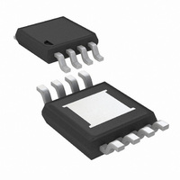
Typical Connection, Pinout, and Package Marking Package Drawing Order Number Package MSOP EXPOSE LME49726MY PAD MSOP EXPOSE LME49726MYX PAD www.national.com FIGURE 2. Inverting Configuration Single Supply Order Number LME49726MY See NS Package Number MUY08A Package Marking 300386x7 Z = Assembly ...
Page 3
... Absolute Maximum Ratings 2) If Military/Aerospace specified devices are required, please contact the National Semiconductor Sales Office/ Distributors for availability and specifications. Power Supply Voltage Storage Temperature Input Voltage (V SS Output Short Circuit (Note 3) Power Dissipation Electrical Characteristics (V the circuit shown in Figure ...
Page 4
Symbol Parameter V Maximum Output Voltage Swing OUTSWING I Output Current OUT I Quiescent Current per Amplifier S Note 1: Absolute Maximum Ratings” indicate limits beyond which damage to the device may occur, including inoperability and degradation of device reliability ...
Page 5
Typical Performance Characteristics THD+N vs Output Voltage V = 1.25V –1.25V – 1kHz 22–22kHz V THD+N vs Output Voltage V = 1.25V –1.25V ...
Page 6
THD+N vs Output Voltage V = 2.50V –2.50V – 1kHz 22–22kHz V THD+N vs Output Voltage V = 2.75V –2.75V –1, f ...
Page 7
PSRR+ vs Frequency V = 1.25V –1.25V 200mV DD SS RIPPLE Input terminated 22–80kHz PSRR+ vs Frequency V = 2.50V –2.50V 200mV DD EE RIPPLE Input terminated 22–80kHz ...
Page 8
Output Voltage vs Supply Voltage = 600Ω 1kHz, THD 22–80kHz Crosstalk vs Frequency V = 2.50V –2.50V – 1kHz 80kHz ...
Page 9
Application Information DISTORTION MEASUREMENTS The vanishingly low residual distortion produced by LME49726 is below the capabilities of all commercially avail- able equipment. This makes distortion measurements just slightly more difficult than simply connecting a distortion me- ter to the amplifier's ...
Page 10
Figure 5 shows the typical connection for a dual supply in- verting amplifier. The output voltage is centered on zero. FIGURE 5. Dual Supply Inverting Configuration www.national.com Figure 6 shows the typical connection for the Buffer Amplifier or also called ...
Page 11
Typical Applications NAB Preamp kHz = 0.38 μ Weighted Balanced to Single Ended Converter V = V1–V2 O NAB Preamp Voltage Gain vs Frequency ...
Page 12
Second Order High Pass Filter (Butterworth) Illustration kHz 0 Illustration kHz 10 www.national.com Second Order Low Pass Filter 300386n9 Illustration kHz ...
Page 13
Channel Panning Circuit (Pan Pot) Illustration is Hz 320 =11 kHz 1.1 kHz H HB 300386o3 Tone Control 300386o5 13 Line Driver 300386o4 300386o6 www.national.com ...
Page 14
0.33 μ S kHz A Weighted A Weighted kHz Illustration is 101(V2 − V1) www.national.com RIAA ...
Page 15
... Note 8: At volume of change = ±12 dB 1.7 Reference: “AUDIO/RADIO HANDBOOK”, National Semiconductor, 1980, Page 2–61 10 Band Graphic Equalizer 0.12μF 4.7μF 32 75kΩ 0.056μF 3.3μF 64 68kΩ 0.033μF 1.5μF 62kΩ ...
Page 16
LME49726 Bill of Materials Description Ceramic Capacitor 0.1uF, 10%, 50V 0805 SMD Tantalum Capacitor 2.2uF,10%, 20V, A-size Tantalum Capacitor 10uF,10%, 20V, B-size Resistor 0Ω, 1/8W 1% 0805 SMD Header, 2-Pin Header, 3-Pin Resistor 10kΩ, 1/8W 1% 0805 SMD Dual Rail-to-Rail ...
Page 17
LME49726 Board Circuit 17 www.national.com ...
Page 18
LME49726 Demo Board Views www.national.com 30038641 Top Silkscreen 300386x9 Top Layer 18 ...
Page 19
Bottom Layer 19 www.national.com ...
Page 20
Revision History Rev 1.0 1.01 www.national.com Date Description 11/05/08 Initial release. 05/25/10 Increased Operating Temperature Range. 20 ...
Page 21
Physical Dimensions inches (millimeters) unless otherwise noted Mini-SOIC Exposed-DAP Package Order Number LME49726MY NS Package Number MUY08A 21 www.national.com ...
Page 22
... For more National Semiconductor product information and proven design tools, visit the following Web sites at: www.national.com Products Amplifiers www.national.com/amplifiers Audio www.national.com/audio Clock and Timing www.national.com/timing Data Converters www.national.com/adc Interface www.national.com/interface LVDS www.national.com/lvds Power Management www.national.com/power Switching Regulators www.national.com/switchers LDOs www.national.com/ldo LED Lighting www ...