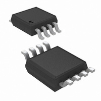
LMH6626MM/NOPB National Semiconductor, LMH6626MM/NOPB Datasheet

LMH6626MM/NOPB
Specifications of LMH6626MM/NOPB
LMH6626MMTR
Available stocks
Related parts for LMH6626MM/NOPB
LMH6626MM/NOPB Summary of contents
Page 1
... The LMH6624/LMH6626 operate from dual supply mode and from +5V to +12V in single supply configuration. LMH6624 is offered in SOT23-5 and SOIC-8 packages. The LMH6626 is offered in SOIC-8 and MSOP-8 packages. Connection Diagrams 5-Pin SOT23 20058951 Top View © 2005 National Semiconductor Corporation Features ± 6V specified) ...
Page 2
... Absolute Maximum Ratings If Military/Aerospace specified devices are required, please contact the National Semiconductor Sales Office/ Distributors for availability and specifications. ESD Tolerance Human Body Model Machine Model V Differential IN + − Supply Voltage ( Voltage at Input pins Soldering Information Infrared or Convection (20 sec.) ± 2.5V Electrical Characteristics Unless otherwise specified, all limits guaranteed at T 100Ω ...
Page 3
Electrical Characteristics Unless otherwise specified, all limits guaranteed at T 100Ω. Boldface limits apply at the temperature extremes. See (Note 12). Symbol Parameter Transfer Characteristics A Large Signal Voltage Gain VOL X Crosstalk Rejection t Output Characteristics V ...
Page 4
Electrical Characteristics Unless otherwise specified, all limits guaranteed at T 100Ω. Boldface limits apply at the temperature extremes. See (Note 12). Symbol Parameter t Fall Time f t Settling Time 0.1% s Distortion and Noise Response e Input ...
Page 5
Electrical Characteristics Unless otherwise specified, all limits guaranteed at T 100Ω. Boldface limits apply at the temperature extremes. See (Note 12). Symbol Parameter I Output Short Circuit Current SC I Output Current OUT Power Supply PSRR Power Supply ...
Page 6
Typical Performance Characteristics Voltage Noise vs. Frequency Inverting Frequency Response Non-Inverting Frequency Response www.national.com Current Noise vs. Frequency 20058962 Inverting Frequency Response 20058989 Non-Inverting Frequency Response 20058904 6 20058963 20058988 20058903 ...
Page 7
Typical Performance Characteristics Open Loop Frequency Response Over Temperature Frequency Response with Cap. Loading Frequency Response with Cap. Loading (Continued) Open Loop Frequency Response Over Temperature 20058966 Frequency Response with Cap. Loading 20058984 Frequency Response with Cap. Loading 20058987 7 ...
Page 8
Typical Performance Characteristics Non-Inverting Frequency Response Varying V Non-Inverting Frequency Response Varying V (LMH6624) Non-Inverting Frequency Response Varying V (LMH6624) www.national.com (Continued) Non-Inverting Frequency Response Varying V IN 20058906 Non-Inverting Frequency Response Varying V IN 20058908 Non-Inverting Frequency Response Varying ...
Page 9
Typical Performance Characteristics Sourcing Current vs. V OUT Sourcing Current vs. V OUT V vs. V (LMH6624) OS SUPPLY (Continued) (LMH6624) Sourcing Current vs. V 20058957 (LMH6624) Sourcing Current vs. V 20058954 20058967 9 (LMH6626) OUT 20058972 (LMH6626) OUT 20058969 ...
Page 10
Typical Performance Characteristics Sinking Current vs. V OUT Sinking Current vs. V OUT I vs SUPPLY www.national.com (Continued) (LMH6624) Sinking Current vs. V 20058958 (LMH6624) Sinking Current vs. V 20058956 Crosstalk Rejection vs. Frequency (LMH6626) 20058953 10 (LMH6626) ...
Page 11
Typical Performance Characteristics Distortion vs. Frequency Distortion vs. Frequency Distortion vs. V Peak to Peak OUT (Continued) Distortion vs. Frequency 20058944 Distortion vs. Gain 20058945 Distortion vs. V 20058943 11 20058946 20058978 Peak to Peak OUT 20058977 www.national.com ...
Page 12
Typical Performance Characteristics Non-Inverting Large Signal Pulse Response Non-Inverting Small Signal Pulse Response PSRR vs. Frequency www.national.com (Continued) Non-Inverting Large Signal Pulse Response 20058973 Non-Inverting Small Signal Pulse Response 20058975 PSRR vs. Frequency 20058948 12 20058974 20058976 20058949 ...
Page 13
Typical Performance Characteristics Input Referred CMRR vs. Frequency Amplifier Peaking with Varying R (Continued) Input Referred CMRR vs. Frequency 20058901 Amplifier Peaking with Varying R F 20058983 13 20058902 F 20058982 www.national.com ...
Page 14
Application Section FIGURE 1. Non-Inverting Amplifier Configuration INTRODUCTION The LMH6624/LMH6626 are very wide gain bandwidth, ultra low noise voltage feedback operational amplifiers. Their ex- cellent performances enable applications such as medical diagnostic ultrasound, magnetic tape & disk storage and fiber-optics ...
Page 15
Application Section (Continued for bias current cancellation. Figure 4 illustrates f g seq the equivalent noise model using this assumption. Figure plot of e against equivalent source resistance (R ni with all of ...
Page 16
Application Section (Continued) noise density (i ) equation for the basic transimpedance ni configuration and is plotted against feedback resistance (R showing all contributing noise sources in Figure 8. This plot indicates the expected total equivalent input current noise density ...
Page 17
... FIGURE 11. Noise Magnetic Media Equalizer FIGURE 12. Equalizer Frequency Response LAYOUT CONSIDERATION National Semiconductor suggests the copper patterns on the evaluation boards listed below as a guide for high frequency layout. These boards are also useful as an aid in device testing and characterization the case with all high- speed amplifiers, accepted-practice RF design technique on the PCB layout is mandatory ...
Page 18
Physical Dimensions www.national.com inches (millimeters) unless otherwise noted 5-Pin SOT23 NS Package Number MF05A 8-Pin SOIC NS Package Number M08A 18 ...
Page 19
... BANNED SUBSTANCE COMPLIANCE National Semiconductor manufactures products and uses packing materials that meet the provisions of the Customer Products Stewardship Specification (CSP-9-111C2) and the Banned Substances and Materials of Interest Specification (CSP-9-111S2) and contain no ‘‘Banned Substances’’ as defined in CSP-9-111S2. ...


