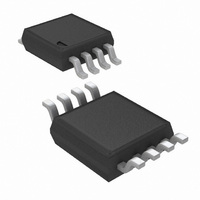
LMP7732MME/NOPB National Semiconductor, LMP7732MME/NOPB Datasheet

LMP7732MME/NOPB
Specifications of LMP7732MME/NOPB
Related parts for LMP7732MME/NOPB
LMP7732MME/NOPB Summary of contents
Page 1
... The LMP7731 is the single version of this product and is of- fered in the 5-Pin SOT-23 and 8-Pin SOIC packages. Typical Performance Characteristics Input Voltage Noise vs. Frequency LMP ® registered trademark of National Semiconductor Corporation. © 2009 National Semiconductor Corporation LMP7732 Features (Typical values, T ■ ...
Page 2
... Absolute Maximum Ratings If Military/Aerospace specified devices are required, please contact the National Semiconductor Sales Office/ Distributors for availability and specifications. ESD Tolerance (Note 2) Human Body Model For inputs pins only For all other pins Machine Model Charge Device Model V Differential IN Supply Voltage ( – ...
Page 3
Symbol Parameter Output Voltage Swing High V OUT Output Voltage Swing Low I Output Current OUT I Supply Current S SR Slew Rate GBW Gain Bandwidth G Gain Margin M Φ Phase Margin M R Input Resistance IN THD+N Total ...
Page 4
Symbol Parameter TCI Input Offset Current Drift OS CMRR Common Mode Rejection Ratio PSRR Power Supply Rejection Ratio CMVR Common Mode Voltage Range A Open Loop Voltage Gain VOL Output Voltage Swing High V OUT Output Voltage Swing Low I ...
Page 5
Electrical Characteristics Unless otherwise specified, all limits are guaranteed for T limits apply at the temperature extremes. Symbol Parameter Input Offset Voltage V OS (Note 7) TCV Input Offset Voltage Temperature Drift OS I Input Bias Current B I ...
Page 6
Symbol Parameter G Gain Margin M Φ Phase Margin M R Input Resistance IN THD+ N Total Harmonic Distortion + Noise Input Referred Voltage Noise Density e n Input Voltage Noise i Input Referred Current Noise Density n Note 1: ...
Page 7
Typical Performance Characteristics Offset Voltage Distribution Offset Voltage Distribution Offset Voltage Distribution Unless otherwise noted: T TCV 30015071 TCV 30015073 TCV 30015070 7 = 25°C, R > 10 kΩ / Distribution OS 30015076 ...
Page 8
Offset Voltage Distribution Offset Voltage vs. Temperature PSRR vs. Frequency www.national.com TCV 30015072 Offset Voltage vs. Temperature 30015082 CMRR vs. Frequency 30015029 8 Distribution OS 30015075 30015083 30015062 ...
Page 9
Offset Voltage vs. Supply Voltage 30015053 Offset Voltage vs 30015055 Input Offset Voltage Time Drift 30015080 Offset Voltage vs. V Offset Voltage vs. V Slew Rate vs. Supply Voltage 9 CM 30015054 CM 30015056 30015020 www.national.com ...
Page 10
Time Domain Voltage Noise Time Domain Voltage Noise Input Bias Current vs. V www.national.com Time Domain Voltage Noise 30015067 Output Voltage vs. Output Current 30015066 Input Bias Current vs 30015025 10 30015065 30015057 CM 30015026 ...
Page 11
Input Bias Current vs 30015027 Open Loop Frequency Response THD+N vs. Frequency 30015085 Open Loop Frequency Response Over Temperature Open Loop Frequency Response 30015019 THD+N vs. Output Voltage 11 30015018 30015028 30015069 www.national.com ...
Page 12
Large Signal Step Response Large Signal Step Response Supply Current vs. Supply Voltage www.national.com Small Signal Step Response 30015022 Small Signal Step Response 30015024 Output Swing High vs. Supply Voltage 30015081 12 30015021 30015023 30015058 ...
Page 13
Output Swing Low vs. Supply Voltage 30015059 Sourcing Current vs. Supply Voltage 30015061 Sinking Current vs, Supply Voltage 13 30015060 www.national.com ...
Page 14
... National Semiconductor is heavily committed to precision amplifiers and the market segment they serve. Technical sup- port and extensive characterization data is available for sen- sitive applications or applications with a constrained error budget ...
Page 15
FIGURE 3. 0 Input Voltage Noise Measuring the very low peak-to-peak noise performance of the LMP7732, requires special testing attention. In order to achieve accurate results, the device should be warmed up for at least five ...
Page 16
DRIVING AN ADC Analog to Digital Converters, ADCs, usually have a sampling capacitor on their input. When the ADC's input is directly con- nected to the output of the amplifier a charging current flows from the amplifier to the ADC. ...
Page 17
Physical Dimensions inches (millimeters) unless otherwise noted 8-Pin SOIC NS Package Number M08A 8-Pin MSOP NS Package Number MUA08A 17 www.national.com ...
Page 18
... For more National Semiconductor product information and proven design tools, visit the following Web sites at: Products Amplifiers www.national.com/amplifiers Audio www.national.com/audio Clock and Timing www.national.com/timing Data Converters www.national.com/adc Interface www.national.com/interface LVDS www.national.com/lvds Power Management www.national.com/power Switching Regulators www.national.com/switchers LDOs www.national.com/ldo LED Lighting www ...


