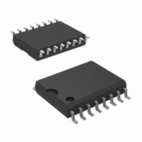
LM614CWM/NOPB National Semiconductor, LM614CWM/NOPB Datasheet

LM614CWM/NOPB
Specifications of LM614CWM/NOPB
*LM614CWM/NOPB
LM614CWM
Related parts for LM614CWM/NOPB
LM614CWM/NOPB Summary of contents
Page 1
... Package Range 16-Pin Wide 0˚C to 70˚C Body SOIC −40˚C to 85˚C Super-Block ™ trademark of National Semiconductor Corporation. © 2001 National Semiconductor Corporation Features Op Amp n Low operating current: n Wide supply voltage range 36V n Wide common-mode range Wide differential input voltage: Reference n Adjustable output voltage: 1 ...
Page 2
... Absolute Maximum Ratings If Military/Aerospace specified devices are required, please contact the National Semiconductor Sales Office/ Distributors for availability and specifications. Voltage on Any Pins except V R − (referred to V pin) (Note 2) (Note 3) Current through Any Input Pin & V Pin R Differential Input Voltage ...
Page 3
Electrical Characteristics − These specifications apply for V = GND = 0V, V unless otherwise specified. Limits in standard typeface are for T Temperature Range . Symbol Parameter A Open Loop V Voltage Gain SR Slew Rate GBW Gain Bandwidth ...
Page 4
Electrical Characteristics − These specifications apply for V = GND = 0V, V unless otherwise specified. Limits in standard typeface are for T Temperature Range . Symbol Parameter Note 1: Absolute maximum ratings indicate limits beyond which damage to the ...
Page 5
Typical Performance Characteristics (Reference) = 0V, unless otherwise noted (Continued) Accelerated Reference Voltage Drift vs. Time Reference Voltage vs. Current and Temperature Reference Voltage vs. Reference Current T Reference Voltage vs. Current and Temperature 00932649 Reference Voltage vs. Reference Current ...
Page 6
Typical Performance Characteristics (Reference) = 0V, unless otherwise noted (Continued) FEEDBACK Current vs. FEEDBACK-to-Anode Voltage Reference Noise Voltage vs. Frequency Reference Power-Up Time www.national.com T J FEEDBACK Current vs. FEEDBACK-to-Anode Voltage 00932655 Reference Small-Signal Resistance vs. Frequency 00932657 Reference Voltage ...
Page 7
Typical Performance Characteristics (Reference) = 0V, unless otherwise noted (Continued) Reference Voltage with 100 12 µA Current Step Reference Voltage Change with Supply Voltage Step Typical Performance Characteristics (Op Amps / 25˚C, unless otherwise ...
Page 8
Typical Performance Characteristics (Op Amps / 25˚C, unless otherwise noted (Continued) OUT J Input Bias Current vs. Common-Mode Voltage Large-Signal Step Response Output Source Current vs. Output Voltage and Temp. www.national.com + V Slew ...
Page 9
Typical Performance Characteristics (Op Amps / 25˚C, unless otherwise noted (Continued) OUT J Output Swing, Large Signal Small-Signal Pulse Response vs. Temp. Op Amp Voltage Noise vs. Frequency + V Output Impedance vs. Frequency ...
Page 10
Typical Performance Characteristics (Op Amps / 25˚C, unless otherwise noted (Continued) OUT J Small-Signal Voltage Gain vs. Frequency and Temperature Follower Small-Signal Frequency Response Power Supply Current vs. Power Supply Voltage www.national.com + V ...
Page 11
Typical Performance Characteristics (Op Amps / 25˚C, unless otherwise noted (Continued) OUT J Negative Power Supply Voltage Rejection Ratio Input Bias Current vs. Junction Temperature Typical Performance Distributions Average V Drift Industrial Temperature Range ...
Page 12
Typical Performance Distributions Average I Drift Industrial Temperature Range OS Voltage Reference Broad-BandNoise Distribution www.national.com (Continued) Average I Drift Commercial Temperature Range OS 00932633 Op Amp Voltage Noise Distribution 00932635 Op Amp Current Noise Distribution 00932637 12 00932634 00932636 ...
Page 13
Application Information VOLTAGE REFERENCE Reference Biasing The voltage reference shunt regulator topology that models as a simple zener diode. With current I “forward” direction there is the familiar diode transfer func- tion. I flowing in the reverse ...
Page 14
Application Information R1 = Vr/I = 1.24/32µ = 39k {(Vro/Vr) − 39k {(5/1.24) − 1)} = 118k FIGURE 5. Resistors R1 and R2 Program Reference Output Voltage Understanding that V is fixed ...
Page 15
Application Information 00932619 FIGURE 11. Negative-TC Current Source Hysteresis The reference voltage depends, slightly, on the thermal his- tory of the die. Competitive micro-power vary — always check the data sheet for any given device. Do not assume that no ...
Page 16
Typical Applications FIGURE 12. Simple Low Quiescent Drain Voltage Regulator. Total supply current approximately 320µA, when V *10k must be low t.c. trimpot. FIGURE 13. Ultra Low Noise 10.00V Reference. Total output noise is typically 14µ /Pe ...
Page 17
Typical Applications (Continued) FIGURE 15. Transducer Data Acquisition System. Set zero code voltage, then adjust 10 scale. 17 00932645 gain adjust pot for full www.national.com ...
Page 18
Simplified Schematic Diagrams www.national.com Op Amp 00932602 Reference / Bias 18 00932603 ...
Page 19
... NATIONAL’S PRODUCTS ARE NOT AUTHORIZED FOR USE AS CRITICAL COMPONENTS IN LIFE SUPPORT DEVICES OR SYSTEMS WITHOUT THE EXPRESS WRITTEN APPROVAL OF THE PRESIDENT AND GENERAL COUNSEL OF NATIONAL SEMICONDUCTOR CORPORATION. As used herein: 1. Life support devices or systems are devices or systems which, (a) are intended for surgical implant ...


