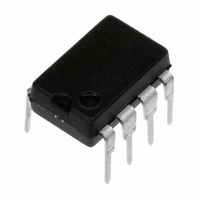
LM6172IN/NOPB National Semiconductor, LM6172IN/NOPB Datasheet

LM6172IN/NOPB
Specifications of LM6172IN/NOPB
LM6172IN
Related parts for LM6172IN/NOPB
LM6172IN/NOPB Summary of contents
Page 1
... LM6171 datasheet for a single amplifier with these same features. LM6172 Driving Capacitive Load Connection Diagram VIP is a trademark of National Semiconductor Corporation. ™ PAL ® registered trademark of and used under license from Advanced Micro Devices, Inc. © 2004 National Semiconductor Corporation ...
Page 2
Ordering Information Package Industrial −40˚C to +85˚C 8-Pin DIP LM6172IN 8-Pin CDIP LM6172AMJ-QML 16-Pin Ceramic LM6172AMWG-QML SOIC 8-Pin LM6172IM Small Outline LM6172IMX www.national.com Temperature Range Military −55˚C to +125˚C 5962-95604 5962-95604 2 Transport Media NSC Drawing Rails N08E Rails J08A ...
Page 3
... Absolute Maximum Ratings If Military/Aerospace specified devices are required, please contact the National Semiconductor Sales Office/ Distributors for availability and specifications. ESD Tolerance (Note 2) Human Body Model Machine Model + − Supply Voltage (V − Differential Input Voltage Common Mode Voltage Range Input Current ...
Page 4
DC Electrical Characteristics Unless otherwise specified, all limits guaranteed for T limits apply at the temperature extremes Symbol Parameter I Output Short Circuit SC Current I Supply Current S ± 15V AC Electrical Characteristics Unless otherwise specified, T ...
Page 5
DC Electrical Characteristics Unless otherwise specified, all limits guaranteed for T its apply at the temperature extremes Symbol Parameter R Input Resistance IN R Output Resistance O CMRR Common Mode Rejection Ratio PSRR Power Supply Rejection Ratio V ...
Page 6
AC Electrical Characteristics Unless otherwise specified 25˚ Symbol Parameter e Input-Referred n Voltage Noise i Input-Referred n Current Noise Second Harmonic Distortion (Note 10) Third Harmonic Distortion (Note 10) Note 1: Absolute Maximum Ratings ...
Page 7
Typical Performance Characteristics Supply Voltage vs. Supply Current Input Offset Voltage vs. Temperature Short Circuit Current vs. Temperature (Sourcing) unless otherwise noted, T Supply Current vs. Temperature 01258114 Input Bias Current vs. Temperature 01258116 Short Circuit Current vs. Temperature (Sinking) ...
Page 8
Typical Performance Characteristics Output Voltage vs. Output Current ± 15V) S CMRR vs. Frequency PSRR vs. Frequency www.national.com unless otherwise noted, T Output Voltage vs. Output Current 01258136 PSRR vs. Frequency 01258119 Open-Loop Frequency Response 01258133 8 = ...
Page 9
Typical Performance Characteristics Open-Loop Frequency Response Large Signal Voltage Gain vs. Load Input Voltage Noise vs. Frequency unless otherwise noted, T Gain-Bandwidth Product vs. Supply Voltage at Different 01258122 Large Signal Voltage Gain vs. Load 01258138 Input Voltage Noise vs. ...
Page 10
Typical Performance Characteristics Input Current Noise vs. Frequency Slew Rate vs. Supply Voltage Large Signal Pulse Response www.national.com unless otherwise noted, T 01258142 01258125 ± 15V 01258102 10 = 25˚C (Continued) A Input ...
Page 11
Typical Performance Characteristics Large Signal Pulse Response ± + Large Signal Pulse Response ± + 15V V S Large Signal Pulse Response ± + ...
Page 12
Typical Performance Characteristics Large Signal Pulse Response A = − Large Signal Pulse Response A = − Closed Loop Frequency Response vs. Supply Voltage (A = +1) V www.national.com unless otherwise noted, ...
Page 13
Typical Performance Characteristics Harmonic Distortion vs. Frequency ± 15V) S Crosstalk Rejection vs. Frequency unless otherwise noted, T Harmonic Distortion vs. Frequency 01258130 Maximum Power Dissipation vs. Ambient Temperature 01258131 13 = 25˚C (Continued) A ± ...
Page 14
LM6172 Simplified Schematic (Each Amplifier) Application Notes LM6172 PERFORMANCE DISCUSSION The LM6172 is a dual high-speed, low power, voltage feed- back amplifier unity-gain stable and offers outstanding performance with only 2.3mA of supply current per channel. The combination ...
Page 15
Application Notes (Continued) FIGURE 2. The LM6172 Driving a 510pF Load with a 30Ω Isolation Resistor FIGURE 3. The LM6172 Driving a 220 pF Load with a 50Ω Isolation Resistor LAYOUT CONSIDERATION PRINTED CIRCUIT BOARDS AND HIGH SPEED OP AMPS ...
Page 16
Application Notes (Continued) POWER SUPPLY BYPASSING Bypassing the power supply is necessary to maintain low power supply impedance across frequency. Both positive and negative power supplies should be bypassed individu- ally by placing 0.01µF ceramic capacitors directly to power supply ...
Page 17
Application Circuits I-to-V Converters 01258148 Differential Line Driver 17 01258149 www.national.com ...
Page 18
Physical Dimensions Order Number LM6172AMJ-QML or 5962-9560401QPA 8-Lead (0.150" Wide) Molded Small Outline Package, JEDEC www.national.com inches (millimeters) unless otherwise noted 8-Lead Ceramic Dual-In-Line Package NS Package Number J08A Order Number LM6172IM or LM6172IMX NS Package Number M08A 18 ...
Page 19
... BANNED SUBSTANCE COMPLIANCE National Semiconductor certifies that the products and packing materials meet the provisions of the Customer Products Stewardship Specification (CSP-9-111C2) and the Banned Substances and Materials of Interest Specification (CSP-9-111S2) and contain no ‘‘Banned Substances’’ as defined in CSP-9-111S2. ...


