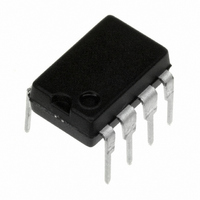
LME49860NA/NOPB National Semiconductor, LME49860NA/NOPB Datasheet - Page 3

LME49860NA/NOPB
Manufacturer Part Number
LME49860NA/NOPB
Description
IC AMP AUDIO STER AB HIFI 8DIP
Manufacturer
National Semiconductor
Datasheet
1.LME49860MABD.pdf
(34 pages)
Specifications of LME49860NA/NOPB
Amplifier Type
Audio
Number Of Circuits
2
Slew Rate
20 V/µs
Gain Bandwidth Product
55MHz
Current - Input Bias
10nA
Voltage - Input Offset
140µV
Current - Supply
10.5mA
Current - Output / Channel
37mA
Voltage - Supply, Single/dual (±)
5 V ~ 44 V, ±2.5 V ~ 22 V
Operating Temperature
-40°C ~ 85°C
Mounting Type
Through Hole
Package / Case
8-DIP (0.300", 7.62mm)
Amplifier Class
AB
No. Of Channels
2
Supply Voltage Range
± 2.5V To ± 22V
Load Impedance
2kohm
Operating Temperature Range
-40°C To +85°C
Amplifier Case Style
DIP
No. Of Pins
8
Rohs Compliant
Yes
Number Of Channels
2
Voltage Gain Db
140 dB
Common Mode Rejection Ratio (min)
110 dB
Input Offset Voltage
0.7 mV at +/- 22 V
Maximum Operating Temperature
+ 85 C
Maximum Dual Supply Voltage
+/- 22 V
Minimum Operating Temperature
- 40 C
For Use With
LME49860NABD - BOARD EVALUATION LME49860NA
Lead Free Status / RoHS Status
Lead free / RoHS Compliant
Output Type
-
-3db Bandwidth
-
Lead Free Status / Rohs Status
Details
Other names
LME49860NA
THD+N
IMD
GBWP
SR
FPBW
t
e
i
V
ΔV
PSRR
ISO
I
ΔI
I
V
n
s
B
OS
n
OS
IN-CM
OS
Absolute Maximum Ratings
If Military/Aerospace specified devices are required,
please contact the National Semiconductor Sales Office/
Distributors for availability and specifications.
Electrical Characteristics for the LME49860
±18V and ±22V, R
Symbol
Power Supply Voltage
Storage Temperature
Input Voltage
Output Short Circuit (Note 3)
ESD Susceptibility (Note 4)
ESD Susceptibility (Note 5)
OS
CH-CH
/ΔTemp
(V
Pins 1, 4, 7 and 8
/ΔTemp
S
= V
+
- V
Total Harmonic Distortion + Noise
Intermodulation Distortion
Gain Bandwidth Product
Slew Rate
Full Power Bandwidth
Settling time
Equivalent Input Noise Voltage
Equivalent Input Noise Density
Current Noise Density
Offset Voltage
Average Input Offset Voltage Drift vs
Temperature
Average Input Offset Voltage Shift vs
Power Supply Voltage
Channel-to-Channel Isolation
Input Bias Current
Input Bias Current Drift vs
Temperature
Input Offset Current
Common-Mode Input Voltage Range
-
)
L
= 2kΩ, R
Parameter
SOURCE
(V-)
= 10Ω, f
-
0.7V to (V+)
−65°C to 150°C
IN
= 1kHz, T
(Notes 1, 2)
Continuous
A
A
Two-tone, 60Hz & 7kHz 4:1
V
referenced to output magnitude
at f = 1kHz
A
0.1% error range
f
f = 1kHz
f = 10Hz
f = 1kHz
f = 10Hz
V
V
–40°C
(Note 8)
V
V
f
f
V
–40°C
V
V
V
BW
IN
IN
+
V
V
OUT
V
S
S
S
S
CM
CM
S
S
2000V
R
R
= 1kHz
= 20kHz
= –1, 10V step, C
= 1, V
= 1, V
= ±18V
= ±22V
= ±18V, Δ V
= ±22V, Δ V
= ±18V
= ±22V
200V
L
L
= 20Hz to 20kHz
0.7V
= 0V
= 0V
46V
= 2kΩ
= 600Ω
= 1V
A
≤
≤
= 25°C, unless otherwise specified.
OUT
OUT
T
T
P-P
A
A
≤
≤
Conditions
3
, –3dB
= 3V
= 3V
85°C
85°C
S
S
= 24V
= 30V
Operating Ratings
rms
RMS
Junction Temperature
Thermal Resistance
θ
θ
Temperature Range
Supply Voltage Range
Pins 2, 3, 5 and 6
T
L
JA
JA
MIN
= 100pF
(SO)
(NA)
(Note 1)
≤
T
A
≤
T
MAX
The following specifications apply for V
(Note 6)
0.00003
0.00003
0.00005
Typical
±0.12
±0.14
+17.1
–16.9
+21.0
–20.8
0.34
±20
120
120
118
112
1.2
2.7
6.4
1.6
3.1
0.2
0.1
55
10
10
11
LME49860
(V+) – 2.0
(V+) – 2.0
(V-) + 2.0
(V-) + 2.0
(Note 7)
0.00009
−40°C
±2.5V
Limit
0.65
±0.7
±0.7
±15
110
4.7
45
72
65
≤
≤
www.national.com
V
T
S
145°C/W
102°C/W
A
MHz (min)
V/μs (min)
≤
mV (max)
mV (max)
≤
nA (max)
nA (max)
% (max)
dB (min)
(Limits)
150°C
V (min)
V (min)
V (min)
V (min)
μV
nV/
pA/
μV/°C
nA/°C
Units
(max)
(max)
100V
±22V
85°C
MHz
dB
dB
μs
%
RMS
S
√
√
=
Hz
Hz


