LMC6464AIM/NOPB National Semiconductor, LMC6464AIM/NOPB Datasheet - Page 16
LMC6464AIM/NOPB
Manufacturer Part Number
LMC6464AIM/NOPB
Description
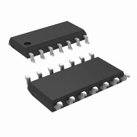
IC OP AMP QUAD MICPWR R-R 14SOIC
Manufacturer
National Semiconductor
Datasheet
1.LMC6462AINNOPB.pdf
(20 pages)
Specifications of LMC6464AIM/NOPB
Amplifier Type
General Purpose
Number Of Circuits
4
Output Type
Rail-to-Rail
Slew Rate
0.028 V/µs
Gain Bandwidth Product
50kHz
Current - Input Bias
0.15pA
Voltage - Input Offset
250µV
Current - Supply
90µA
Current - Output / Channel
75mA
Voltage - Supply, Single/dual (±)
3 V ~ 15.5 V, ±1.5 V ~ 7.75 V
Operating Temperature
-40°C ~ 85°C
Mounting Type
Surface Mount
Package / Case
14-SOIC (3.9mm Width), 14-SOL
Number Of Channels
4
Voltage Gain Db
129.54 dB
Common Mode Rejection Ratio (min)
70 dB
Input Voltage Range (max)
15.5 V
Input Voltage Range (min)
3 V
Input Offset Voltage
0.5 mV at 5 V
Operating Supply Voltage
5 V, 9 V, 12 V, 15 V
Supply Current
0.11 mA at 5 V
Maximum Operating Temperature
+ 85 C
Mounting Style
SMD/SMT
Minimum Operating Temperature
- 40 C
Lead Free Status / RoHS Status
Lead free / RoHS Compliant
-3db Bandwidth
-
Lead Free Status / Rohs Status
Details
Other names
*LMC6464AIM
*LMC6464AIM/NOPB
LMC6464AIM
*LMC6464AIM/NOPB
LMC6464AIM


www.national.com
Typical Single-Supply Applications
PRECISION CURRENT SOURCE
The output current I
OSCILLATORS
For single supply 5V operation, the output of the circuit will
swing from 0V to 5V. The voltage divider set up R
R
move from 1.67V (
behaves as the threshold voltage.
R
frequency of oscillation, f
where ∆t is the time the amplifier input takes to move from
1.67V to 3.33V. The calculations are shown below.
where τ = RC = 0.68 seconds
(Continued)
4
1
and C
will cause the non-inverting input of the LMC6462 to
FIGURE 21. 1 Hz Square-Wave Oscillator
FIGURE 20. Precision Current Source
1
determine the time constant of the circuit. The
1
⁄
3
OUT
of 5V) to 3.33V (
is given by:
OSC
is
2
⁄
3
of 5V). This voltage
01205126
01205127
2
, R
3
and
16
→ t
and
→ t
Then,
= 1 Hz
LOW FREQUENCY NULL
Output offset voltage is the error introduced in the output
voltage due to the inherent input offset voltage V
amplifier.
Output Offset Voltage = (Input Offset Voltage) (Gain)
In the above configuration, the resistors R
mine the nominal voltage around which the input signal, V
should be symmetrical. The high frequency component of
the input signal V
quency component will be nulled since the DC level of the
output will be the input offset voltage of the LMC6462 plus
the bias voltage. This implies that the output offset voltage
due to the top amplifier will be eliminated.
1
2
= 0.27 seconds.
= 0.75 seconds
FIGURE 22. High Gain Amplifier
with Low Frequency Null
IN
will be unaffected while the low fre-
5
and R
OS
6
01205128
, of an
deter-
IN
Related parts for LMC6464AIM/NOPB
Image
Part Number
Description
Manufacturer
Datasheet
Request
R

Part Number:
Description:
National Semiconductor [8-Bit D/A Converter]
Manufacturer:
National Semiconductor
Datasheet:
Part Number:
Description:
National Semiconductor [Media Coprocessor]
Manufacturer:
National Semiconductor
Datasheet:
Part Number:
Description:
Digitally Controlled Tone and Volume Circuit with Stereo Audio Power Amplifier, Microphone Preamp Stage and National 3D Sound
Manufacturer:
National Semiconductor
Datasheet:
Part Number:
Description:
Digitally Controlled Tone and Volume Circuit with Stereo Audio Power Amplifier, Microphone Preamp Stage and National 3D Sound
Manufacturer:
National Semiconductor
Datasheet:
Part Number:
Description:
AC97 Rev 2 Codec with Sample Rate Conversion and National 3D Sound
Manufacturer:
National Semiconductor
Part Number:
Description:
Manufacturer:
National Semiconductor
Datasheet:
Part Number:
Description:
Manufacturer:
National Semiconductor
Datasheet:
Part Number:
Description:
General Purpose, Low Voltage, Low Power, Rail-to-Rail Output Operational Amplifiers
Manufacturer:
National Semiconductor
Datasheet:
Part Number:
Description:
8-bit 20 MSPS flash A/D converter.
Manufacturer:
National Semiconductor
Datasheet:
Part Number:
Description:
Low Noise Quad Operational Amplifier
Manufacturer:
National Semiconductor
Datasheet:
Part Number:
Description:
Quad Differential Line Receivers
Manufacturer:
National Semiconductor
Datasheet:
Part Number:
Description:
Quad High Speed Trapezoidal? Bus Transceiver
Manufacturer:
National Semiconductor
Datasheet:
Part Number:
Description:
Dual Line Receiver
Manufacturer:
National Semiconductor
Datasheet:
Part Number:
Description:
TTL to 10k ECL Level Translator with Latch
Manufacturer:
National Semiconductor
Datasheet: