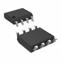
LMP2022MA/NOPB National Semiconductor, LMP2022MA/NOPB Datasheet

LMP2022MA/NOPB
Specifications of LMP2022MA/NOPB
LMP2022MA
Related parts for LMP2022MA/NOPB
LMP2022MA/NOPB Summary of contents
Page 1
... The LMP2021 is offered in 5-Pin SOT-23 and 8-Pin SOIC packages. The LMP2022 is offered in 8-Pin MSOP and 8-Pin SOIC packages. Typical Application The LMP2021/LMP2022 support systems with bits of accuracy. LMP ® registered trademark of National Semiconductor Corporation. © 2009 National Semiconductor Corporation LMP2021/LMP2022 Features (Typical Values, T ■ Input offset voltage (typical) ■ ...
Page 2
... Absolute Maximum Ratings If Military/Aerospace specified devices are required, please contact the National Semiconductor Sales Office/ Distributors for availability and specifications. ESD Tolerance (Note 2) Human Body Model Machine Model Charge Device Model V Differential IN Supply Voltage ( – V − All Other Pins Output Short-Circuit Duration to V ...
Page 3
Symbol Parameter V Output Swing High OUT Output Swing Low I Linear Output Current OUT I Supply Current S SR Slew Rate (Note 10) GBW Gain Bandwidth Product G Gain Margin M Φ Phase Margin M C Input Capacitance IN ...
Page 4
Symbol Parameter EMIRR Electro-Magnetic Interference Rejection Ratio (Note 9) PSRR Power Supply Rejection Ratio A Large Signal Voltage Gain VOL V Output Swing High OUT Output Swing Low I Linear Output Current OUT I Supply Current S SR Slew Rate ...
Page 5
Note 1: Absolute Maximum Ratings indicate limits beyond which damage to the device may occur. Operating Ratings indicate conditions for which the device is intended to be functional, but specific performance is not guaranteed. For guaranteed specifications and the test ...
Page 6
Typical Performance Characteristics Offset Voltage Distribution Offset Voltage Distribution Offset Voltage vs. Supply Voltage www.national.com Unless otherwise noted: T TCV 30014912 TCV 30014913 PSRR vs. Frequency 30014905 6 = 25°C, ...
Page 7
Input Bias Current vs Offset Voltage vs Supply Current vs. Supply Voltage (Per Amplifier) Input Bias Current vs. V 30014962 Offset Voltage vs. V 30014906 Input Voltage Noise vs. Frequency 30014904 7 CM 30014961 CM 30014907 ...
Page 8
Open Loop Frequency Response Open Loop Frequency Response Over Temperature EMIRR vs. Input Power www.national.com Open Loop Frequency Response 30014922 EMIRR vs. Frequency 30014923 EMIRR vs. Input Power 30014932 8 30014921 30014934 30014933 ...
Page 9
Time Domain Input Voltage Noise CMRR vs. Frequency Output Swing High vs. Supply Voltage Time Domain Input Voltage Noise 30014928 Slew Rate vs. Supply Voltage 30014931 Output Swing Low vs. Supply Voltage 30014909 9 30014929 30014916 30014911 www.national.com ...
Page 10
Output Swing High vs. Supply Voltage Overload Recovery Time Large Signal Step Response www.national.com Output Swing Low vs. Supply Voltage 30014908 Overload Recovery Time 30014942 Small Signal Step Response 30014920 10 30014910 30014943 30014918 ...
Page 11
Large Signal Step Response 30014919 Output Voltage vs. Output Current 30014924 Small Signal Step Response Cross Talk Rejection Ratio vs. Frequency (LMP2022) 11 30014917 30014973 www.national.com ...
Page 12
Application Information LMP2021/LMP2022 The LMP2021/LMP2022 are single and dual precision oper- ational amplifiers with ultra low offset voltage, ultra low offset voltage drift, and very low input voltage noise with no 1/f and extended supply voltage range. The LMP2021/LMP2022 of- ...
Page 13
ACHIEVING LOWER NOISE WITH FILTERING The low input voltage noise of the LMP2021/LMP2022, and no 1/f noise make these suitable for many applications with noise sensitive designs. Simple filtering can be done on the LMP2021/LMP2022 to remove high frequency noise. ...
Page 14
Table 1: RMS Input Noise Performance RMS Input Noise (nV) System Amplifier Bandwidth LMP2021/LMP2022 Gain Requirement (V/V) Figure 3 (Hz) Circuit 100 229 10 1000 763 100 229 100 1000 763 10 71 1000 100 158 1000 608 * No ...
Page 15
In a typical I-V converter, the output voltage will be the sum of DC offset plus bias current and the applied signal through the feedback resistor conventional input stage, the in- verting input's capacitance has very little effect ...
Page 16
C in Figure 10 adds a zero to the low pass filter and hence IN eliminating the reduction the LMP2021/LMP2022. VOL An alternative circuit to achieve this is shown in Figure 11. FIGURE 11. Alternative Sensor Impedance ...
Page 17
FIGURE 12. LMP2021/LMP2022 used with ADC161S626 17 30014972 www.national.com ...
Page 18
Physical Dimensions www.national.com inches (millimeters) unless otherwise noted 5-Pin SOT-23 NS Package Number MF05A 8-Pin SOIC NS Package Number M08A 18 ...
Page 19
MSOP NS Package Number MUA08A 19 www.national.com ...
Page 20
... For more National Semiconductor product information and proven design tools, visit the following Web sites at: Products Amplifiers www.national.com/amplifiers Audio www.national.com/audio Clock and Timing www.national.com/timing Data Converters www.national.com/adc Interface www.national.com/interface LVDS www.national.com/lvds Power Management www.national.com/power Switching Regulators www.national.com/switchers LDOs www.national.com/ldo LED Lighting www ...


