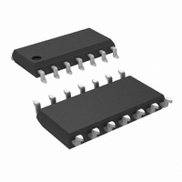
LMP7709MA/NOPB National Semiconductor, LMP7709MA/NOPB Datasheet - Page 19

LMP7709MA/NOPB
Manufacturer Part Number
LMP7709MA/NOPB
Description
IC AMP RRIO PREC QUAD 14SOIC
Manufacturer
National Semiconductor
Series
LMP®, PowerWise®r
Datasheet
1.LMP7707MFNOPB.pdf
(26 pages)
Specifications of LMP7709MA/NOPB
Amplifier Type
General Purpose
Number Of Circuits
4
Output Type
Rail-to-Rail
Slew Rate
5.9 V/µs
Gain Bandwidth Product
15MHz
Current - Input Bias
0.2pA
Voltage - Input Offset
37µV
Current - Supply
3.2mA
Current - Output / Channel
86mA
Voltage - Supply, Single/dual (±)
2.7 V ~ 12 V, ±1.35 V ~ 6 V
Operating Temperature
-40°C ~ 125°C
Mounting Type
Surface Mount
Package / Case
14-SOIC (3.9mm Width), 14-SOL
Lead Free Status / RoHS Status
Lead free / RoHS Compliant
-3db Bandwidth
-
Other names
*LMP7709MA/NOPB
LMP7709MA
LMP7709MA
This example, represented by Figure 8 and Figure 9, is gener-
ic in the sense that the G
between inverting and non-inverting configurations.
The technique of reducing loop gain to stabilize a decompen-
sated op amp circuit will be illustrated using the non-inverting
input configuration shown in Figure 12.
The effect of the choice of resistor R
closed loop gain can be analyzed in the following manner:
Assume the voltage at the inverting input of the op amp is
V
Where G is the open loop gain of the op amp.
Combining Equation 10, Equation 11, and Equation 9 pro-
duces the following equation for closed loop gain,
X
FIGURE 11. Compensation with Reduced Loop Gain
. Then,
FIGURE 12. Closed Loop Gain Analysis with R
MIN
as specified did not distinguish
C
in Figure 12 on the
20203798
202037a3
C
(10)
(11)
(12)
19
By inspection of Equation 12, R
closed loop gain. In this example where R
loop gain remains at 6 dB as long as GF >> 1. The closed
loop gain curve is shown as the solid line in Figure 11.
The addition of R
1. 1/F is moved to a higher gain, resulting in overall system
However, adding R
creased noise gain. The noise gain is defined as the inverse
of the feedback factor, F. The noise gain is the gain from the
amplifier input referred noise to the output. In effect, loop gain
is traded for stability.
2. The ideal closed loop gain retains the same value as the
LEAD-LAG COMPENSATION
This section presents a more advanced compensation tech-
nique that can be used to stabilize amplifiers. The increased
noise gain of the prior circuit is prevented by reducing the low
frequency attenuation of the feedback circuit. This compen-
sation method is called Lead-Lag compensation. Lead-lag
compensation components will be analyzed and a design ex-
ample using this procedure will be discussed.
The feedback function in a lead-lag compensation circuit is
shaped using a resistor and a capacitor. They are chosen in
a way that ensures sufficient phase margin.
Figure 13 shows a Bode plot containing: the open loop gain
of the decompensated amplifier, a feedback function without
compensation and a feedback function with lead-lag com-
pensation.
FIGURE 13. Bode Plot of Open Loop gain G and 1/F with
The shaped feedback function presented in Figure 13 can be
realized using the amplifier configuration in Figure 14. Note
that resistor R
voltage caused by the I
duce more freedom for calculating the lead-lag components.
This will be discussed later in this section.
stability.
circuit without the compensation resistor R
and without Lead-Lag Compensation
P
is only used for compensation of the input
C
affects the circuit in the following ways:
C
results in reduced loop gain and in-
BIAS
current. R
C
does not affect the ideal
P
can be used to intro-
F
= R
C
.
1
www.national.com
, the closed
202037a5


