LM2902NG ON Semiconductor, LM2902NG Datasheet
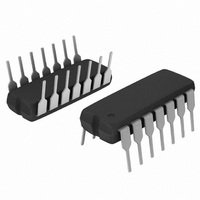
IC OPAMP QUAD SGL SUPPLY 14DIP

LM2902NG

Manufacturer Part Number
LM2902NG
Description
IC OPAMP QUAD SGL SUPPLY 14DIP
Manufacturer
ON Semiconductor
Datasheets

Specifications of LM2902NG

Amplifier Type
General Purpose
Number Of Circuits
4
Slew Rate
0.6 V/µs
Gain Bandwidth Product
1MHz
Current - Input Bias
90nA
Voltage - Input Offset
2000µV
Current - Supply
1.4mA
Current - Output / Channel
40mA
Voltage - Supply, Single/dual (±)
3 V ~ 32 V, ±1.5 V ~ 16 V
Operating Temperature
-40°C ~ 105°C
Mounting Type
Through Hole
Package / Case
14-DIP (0.300", 7.62mm)
Number Of Channels
4
Common Mode Rejection Ratio (min)
50 dB
Input Voltage Range (max)
Positive Rail - 5.7 V
Input Voltage Range (min)
Negative Rail
Input Offset Voltage
7 mV
Input Bias Current (max)
250 nA
Output Current (typ)
40 mA
Operating Supply Voltage
32 V
Supply Current
1.2 mA
Maximum Operating Temperature
+ 105 C
Minimum Operating Temperature
- 40 C
Dual Supply Voltage
+/- 3 V, +/- 5 V, +/- 9 V
Maximum Dual Supply Voltage
+/- 16 V
Minimum Dual Supply Voltage
+/- 1.5 V
Mounting Style
Through Hole
Shutdown
No
Supply Voltage (max)
32 V
Supply Voltage (min)
3 V
Technology
Bipolar
Voltage Gain Db
100 dB
Bandwidth
1 MHz
Channel Separation
-120
Common Mode Rejection Ratio
70
Current, Input Bias
-500 nA
Current, Input Offset
200 nA
Current, Output
40 mA
Current, Supply
3 mA
Number Of Amplifiers
Quad
Package Type
PDIP-14
Temperature, Operating, Range
-40 to +105 °C
Voltage, Gain
15 V/mV
Voltage, Input
-0.3 to 32 VDC
Voltage, Offset
10 mV
Voltage, Output, High
3.5 V
Voltage, Output, Low
5 mV
Voltage, Supply
3 to 32 VDC
Lead Free Status / RoHS Status
Lead free / RoHS Compliant
Output Type
-
-3db Bandwidth
-
Lead Free Status / Rohs Status
Lead free / RoHS Compliant
Other names
LM2902NGOS
LM324, LM324A, LM224,
LM2902, LM2902V, NCV2902
Single Supply Quad
Operational Amplifiers
true differential inputs. They have several distinct advantages over
standard operational amplifier types in single supply applications. The
quad amplifier can operate at supply voltages as low as 3.0 V or as
high as 32 V with quiescent currents about one−fifth of those
associated with the MC1741 (on a per amplifier basis). The common
mode input range includes the negative supply, thereby eliminating the
necessity for external biasing components in many applications. The
output voltage range also includes the negative power supply voltage.
Features
© Semiconductor Components Industries, LLC, 2010
December, 2010 − Rev. 24
The LM324 series are low−cost, quad operational amplifiers with
Device Operation
and Control Changes
Compliant
Short Circuited Protected Outputs
True Differential Input Stage
Single Supply Operation: 3.0 V to 32 V
Low Input Bias Currents: 100 nA Maximum (LM324A)
Four Amplifiers Per Package
Internally Compensated
Common Mode Range Extends to Negative Supply
Industry Standard Pinouts
ESD Clamps on the Inputs Increase Ruggedness without Affecting
NCV Prefix for Automotive and Other Applications Requiring Site
These Devices are Pb−Free, Halogen Free/BFR Free and are RoHS
1
See detailed ordering and shipping information in the package
dimensions section on page 10 of this data sheet.
See general marking information in the device marking
section on page 11 of this data sheet.
DEVICE MARKING INFORMATION
14
Inputs 1
Inputs 2
14
14
Out 1
Out 2
ORDERING INFORMATION
V
1
CC
PIN CONNECTIONS
http://onsemi.com
1
2
3
4
5
6
7
1
*
)
)
*
1
1
2
(Top View)
Publication Order Number:
4
3
*
)
)
*
DTB SUFFIX
CASE 751A
CASE 948G
TSSOP−14
CASE 646
N SUFFIX
D SUFFIX
SOIC−14
PDIP−14
14
13
12
10
11
9
8
Out 4
V
Out 3
EE
Inputs 4
Inputs 3
, GND
LM324/D

Related parts for LM2902NG

LM2902NG Summary of contents

Page 1

LM324, LM324A, LM224, LM2902, LM2902V, NCV2902 Single Supply Quad Operational Amplifiers The LM324 series are low−cost, quad operational amplifiers with true differential inputs. They have several distinct advantages over standard operational amplifier types in single supply applications. The quad amplifier ...

Page 2

MAXIMUM RATINGS ( 25°C, unless otherwise noted.) A Rating Power Supply Voltages Single Supply Split Supplies Input Differential Voltage Range (Note 1) Input Common Mode Voltage Range (Note 2) Output Short Circuit Duration Junction Temperature Thermal Resistance, Junction−to−Air ...

Page 3

ELECTRICAL CHARACTERISTICS LM224 Characteristics Symbol Min Typ Input Offset Voltage 5 ICR V −1 1 ...

Page 4

ELECTRICAL CHARACTERISTICS LM224 Characteristics Symbol Min Typ Output Voltage − High Limit 3 2.0 kW 25° 2.0 kW ...

Page 5

Q16 Q19 5 Q20 Q18 Inputs - Q21 Q17 Q26 Figure 1. Representative Circuit Diagram Q15 Q14 Q13 40 k Q12 25 Q11 Q10 (One−Fourth of Circuit Shown) http://onsemi.com 5 ...

Page 6

The LM324 series is made using four internally compensated, two−stage operational amplifiers. The first stage of each consists of differential input devices Q20 and Q18 with input buffer transistors Q21 and Q17 and the differential to single ended converter Q3 ...

Page 7

Negative 8.0 Positive 6.0 4.0 2 2.0 4.0 6.0 8 ± POWER SUPPLY VOLTAGES (V) CC EE, Figure 5. Input Voltage Range ...

Page 8

1/4 LM324 MC1403 + 2 2 Figure 11. Voltage Reference 1/4 LM324 - - LM324 + ...

Page 9

Triangle Wave ref CC 2 Output V + ref R3 1/4 LM324 100 k V ref ...

Page 10

... LM324NG LM324ADG LM324ADR2G LM324ADTBG LM324ADTBR2G LM324ANG LM2902DG LM2902DR2G LM2902DTBG LM2902DTBR2G LM2902NG LM2902VDG LM2902VDR2G LM2902VDTBG LM2902VDTBR2G LM2902VNG NCV2902DR2G NCV2902DTBR2G †For information on tape and reel specifications, including part orientation and tape sizes, please refer to our Tape and Reel Packaging Specifications Brochure, BRD8011/D. Operating Temperature Range − ...

Page 11

MARKING DIAGRAMS 14 14 LM324AN LMx24N AWLYYWWG AWLYYWWG LM324ADG LMx24DG AWLYWW AWLYWW x24 324A ALYWG ALYWG WL, L YY (Note: ...

Page 12

−T− SEATING PLANE 0.13 (0.005) PACKAGE DIMENSIONS PDIP−14 CASE 646−06 ISSUE http://onsemi.com 12 NOTES: 1. DIMENSIONING AND TOLERANCING PER ANSI ...

Page 13

... G −T− SEATING 14 PL PLANE 0.25 (0.010 14X 0.58 *For additional information on our Pb−Free strategy and soldering details, please download the ON Semiconductor Soldering and Mounting Techniques Reference Manual, SOLDERRM/D. PACKAGE DIMENSIONS SOIC−14 CASE 751A−03 ISSUE 0.25 (0.010 ...

Page 14

... S A −V− C 0.10 (0.004) −T− G SEATING D PLANE 14X 0.36 *For additional information on our Pb−Free strategy and soldering details, please download the ON Semiconductor Soldering and Mounting Techniques Reference Manual, SOLDERRM/D. PACKAGE DIMENSIONS TSSOP−14 CASE 948G−01 ISSUE 0.25 (0.010) ...

Page 15

... Opportunity/Affirmative Action Employer. This literature is subject to all applicable copyright laws and is not for resale in any manner. PUBLICATION ORDERING INFORMATION LITERATURE FULFILLMENT: Literature Distribution Center for ON Semiconductor P.O. Box 5163, Denver, Colorado 80217 USA Phone: 303−675−2175 or 800−344−3860 Toll Free USA/Canada Fax: 303− ...

Related keywords