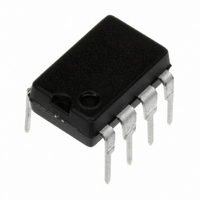
LM4250CN/NOPB National Semiconductor, LM4250CN/NOPB Datasheet

LM4250CN/NOPB
Specifications of LM4250CN/NOPB
*LM4250CN/NOPB
LM4250
LM4250CN
Related parts for LM4250CN/NOPB
LM4250CN/NOPB Summary of contents
Page 1
... LM4250. Connection Diagrams Metal Can Package Top View X5 Difference Amplifier Quiescent © 2000 National Semiconductor Corporation Features ± ± 18V power supply operation input offset current n Standby power consumption as low as 500 nW ...
Page 2
... Absolute Maximum Ratings If Military/Aerospace specified devices are required, please contact the National Semiconductor Sales Office/ Distributors for availability and specifications. (Note 3) Supply Voltage Operating Temp. Range Differential Input Voltage Input Voltage (Note 2) I Current SET Output Short Circuit Duration T JMAX H-Package ...
Page 3
Resistor Biasing Set Current Setting Resistor ± 1.5V 25.6 M ± 3.0V 55.6 M ± 6.0V ± 9.0V ± 12.0V ± 15.0V Electrical Characteristics LM4250 (−55˚C T +125˚C unless otherwise specified Parameter V OS ...
Page 4
Electrical Characteristics Parameter Large Signal Voltage Gain Output Voltage Swing Common Mode Rejection Ratio Supply Voltage Rejection Ratio Supply Current Power Consumption Electrical Characteristics LM4250C (0˚C T +70˚C unless otherwise specified Parameter bias ...
Page 5
Electrical Characteristics Parameter Input Voltage Range Large Signal Voltage Gain Output Voltage Swing Common Mode Rejection Ratio Supply Voltage Rejection Ratio Supply Current Power Consumption Typical Performance Characteristics Input Bias Current vs I SET DS009300-15 Unnulled Input Offset Voltage Change ...
Page 6
Typical Performance Characteristics Peak to Peak Output Voltage Swing vs Supply Voltage DS009300-21 Slew Rate vs I SET DS009300-24 Phase Margin vs I SET DS009300-27 www.national.com (Continued) Quiescent Current ( Temperature DS009300-22 Gain Bandwidth Product vs I ...
Page 7
Typical Applications X5 Difference Amplifier Quiescent Quiescent P = 1.8 µW D *Meter movement (0–100 µ marked for 0–100 nA full scale. 500 Nano-Watt X10 Amplifier DS009300-3 Quiescent P = 500 nW ...
Page 8
Typical Applications (Continued) Note 5: Quiescent µW. D Note 6: R2, R3, R4, R5, R6 and R7 are 1% resistors. Note 7: R11 and C1 are for DC and AC common mode rejection adjustments. − R Connected ...
Page 9
Schematic Diagram Ordering Information Temperature Range Military Commercial −55˚C T +125˚C 0˚ LM4250CN LM4250CM LM4250CMX LM4250J-MIL LM4250CH Package NSC Package +70˚C Number 8-Pin N08E Molded DIP 8-Pin M08A Surface Mount 8-Pin J08E Ceramic DIP 8-Pin H08C Metal ...
Page 10
Physical Dimensions www.national.com inches (millimeters) unless otherwise noted Metal Can Package (H) Order Number LM4250CH NS Package Number H08C Ceramic Dual-In-Line Package (J) Order Number LM4250J-MIL NS Package Number J08A 10 ...
Page 11
Physical Dimensions inches (millimeters) unless otherwise noted (Continued) Small Outline Package (M) Order Number LM4250CM or LM4250CMX NS Package Number M08A Molded Dual-In-Line Package (N) Order Number LM4250CN NS Package Number N08E 11 www.national.com ...
Page 12
... NATIONAL’S PRODUCTS ARE NOT AUTHORIZED FOR USE AS CRITICAL COMPONENTS IN LIFE SUPPORT DEVICES OR SYSTEMS WITHOUT THE EXPRESS WRITTEN APPROVAL OF THE PRESIDENT AND GENERAL COUNSEL OF NATIONAL SEMICONDUCTOR CORPORATION. As used herein: 1. Life support devices or systems are devices or systems which, (a) are intended for surgical implant ...


