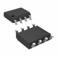
LMP8602MA/NOPB National Semiconductor, LMP8602MA/NOPB Datasheet - Page 18

LMP8602MA/NOPB
Manufacturer Part Number
LMP8602MA/NOPB
Description
IC AMP CURRENT SENSE 60V 8SOIC
Manufacturer
National Semiconductor
Series
LMP®r
Type
Current Sense Amplifierr
Datasheet
1.LMP8602MMENOPB.pdf
(24 pages)
Specifications of LMP8602MA/NOPB
Amplifier Type
Current Sense
Number Of Circuits
1
Slew Rate
0.83 V/µs
Gain Bandwidth Product
60kHz
Current - Input Bias
0.04pA
Voltage - Input Offset
150µV
Current - Supply
1.1mA
Current - Output / Channel
48mA
Voltage - Supply, Single/dual (±)
3 V ~ 5.5 V
Operating Temperature
-40°C ~ 125°C
Mounting Type
Surface Mount
Package / Case
8-SOIC (3.9mm Width)
No. Of Amplifiers
1
Input Bias Current
20nA
Input Offset Voltage
1mV
Bandwidth
60kHz
Cmrr
105dB
Supply Voltage Range
3V To 5.5V
Supply Current
1.3mA
Rohs Compliant
Yes
Number Of Channels
1
Number Of Elements
2
Power Supply Requirement
Single
Common Mode Rejection Ratio
80dB
Voltage Gain Db
34.02dB
Single Supply Voltage (typ)
5V
Dual Supply Voltage (typ)
Not RequiredV
Power Supply Rejection Ratio
70dB
Rail/rail I/o Type
No
Single Supply Voltage (min)
3V
Single Supply Voltage (max)
5.5V
Dual Supply Voltage (min)
Not RequiredV
Dual Supply Voltage (max)
Not RequiredV
Operating Temp Range
-40C to 125C
Operating Temperature Classification
Automotive
Mounting
Surface Mount
Pin Count
8
Package Type
SOIC N
Lead Free Status / RoHS Status
Lead free / RoHS Compliant
Output Type
-
-3db Bandwidth
-
Lead Free Status / Rohs Status
Compliant
Other names
LMP8602MA
Available stocks
Company
Part Number
Manufacturer
Quantity
Price
Company:
Part Number:
LMP8602MA/NOPB
Manufacturer:
National Semiconductor
Quantity:
135
www.national.com
BIDIRECTIONAL CURRENT SENSING
The signal on the A1 and OUT pins is ground-referenced
when the OFFSET pin is connected to ground. This means
that the output signal can only represent positive values of the
current through the shunt resistor, so only currents flowing in
one direction can be measured. When the offset pin is tied to
the positive supply rail, the signal on the A1 and OUT pins is
referenced to a mid-rail voltage which allows bidirectional
current sensing. When the offset pin is connected to a voltage
source, the output signal will be level shifted to that voltage
divided by two. In principle, the output signal can be shifted
to any voltage between 0 and V
voltage from a low impedance source
SET pin.
With the offset pin connected to the supply pin (V
ation of the amplifier will be fully bidirectional and symmetrical
around 0V differential at the input pins. The signal at the out-
put will follow this voltage difference multiplied by the gain and
at an offset voltage at the output of half V
Example:
With 5V supply and a gain of 50x for the LMP8602, a differ-
ential input signal of +10 mV will result in 3.0V at the output
pin. similarly -10 mV at the input will result in 2.0V at the output
pin.
With 5V supply and a gain of 100x for the LMP8603, a differ-
ential input signal of +10 mV will result in 3.5V at the output
pin. similarly -10 mV at the input will result in 1.5V at the output
pin.
Note 16: The OFFSET pin has to be driven from a very low-impedance
source (<10Ω). This is because the OFFSET pin internally connects directly
to the resistive feedback networks of the two gain stages. When the OFFSET
pin is driven from a relatively large impedance (e.g. a resistive divider
between the supply rails) accuracy will decrease.
POWER SUPPLY DECOUPLING
In order to decouple the LMP8602/LMP8602Q/LMP8603/LM-
P8603Q from AC noise on the power supply, it is recom-
mended to use a 0.1 µF bypass capacitor between the V
GND pins. This capacitor should be placed as close as pos-
sible to the supply pins. In some cases an additional 10 µF
bypass capacitor may further reduce the supply noise.
LAYOUT CONSIDERATIONS
The two input signals of the LMP8602/LMP8602Q/LMP8603/
LMP8603Q are differential signals and should be handled as
a differential pair. For optimum performance these signals
should be closely together and of equal length. Keep all
impedances in both traces equal and do not allow any other
signal or ground in between the traces of this signals.
The connection between the preamplifier and the output
buffer amplifier is a high impedance signal due to the 100
kΩ series resistor at the output of the preamplifier. Keep the
traces at this point as short as possible and away from inter-
fering signals.
The LMP8602/LMP8602Q/LMP8603/LMP8603Q is available
in a 8–Pin SOIC package and in a 8–Pin MSOP package. For
the MSOP package, the bare board spacing at the solder
pads of the package will be too small for reliable use at higher
voltages (V
add a conformal coating on the PCB assembled with the
LMP8602/LMP8602Q/LMP8603/LMP8603Q in MSOP pack-
age.
DRIVING SWITCHED CAPACITIVE LOADS
Some ADCs load their signal source with a sample and hold
capacitor. The capacitor may be discharged prior to being
CM
> 25V) In this situation it is strongly advised to
S
/2 by applying twice that
(Note
S
.
16) to the OFF-
S
) the oper-
S
and
18
connected to the signal source. If the LMP8602/LMP8602Q/
LMP8603/LMP8603Q is driving such ADCs the sudden cur-
rent that should be delivered when the sampling occurs may
disturb the output signal. This effect was simulated with the
circuit shown in
capacitor that is driven by a rail to rail square wave.
This circuit simulates the switched connection of a discharged
capacitor to the LMP8602/LMP8602Q/LMP8603/LMP8603Q
output. The resulting V
Figure 7
FIGURE 7. Capacitive Load Response at 3.3V
FIGURE 8. Capacitive Load Response at 5.0V
FIGURE 6. Driving Switched Capacitive Load
and
Figure
Figure 6
8.
OUT
where the output is connected to a
disturbance signals are shown in
30083430
30083431
30083460


