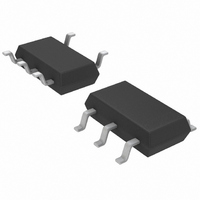
LTC2050HVHS5#TRM Linear Technology, LTC2050HVHS5#TRM Datasheet

LTC2050HVHS5#TRM
Specifications of LTC2050HVHS5#TRM
Available stocks
Related parts for LTC2050HVHS5#TRM
LTC2050HVHS5#TRM Summary of contents
Page 1
... The LTC2050 also features a 1.5μV bandwidth product. L, LT, LTC, LTM, Linear Technology and the Linear logo are registered trademarks of Linear Technology Corporation. ThinSOT is a trademark of Linear Technology Corporation. All other trademarks are the property of their respective owners. Protected by U.S. Patents, including 5481178 ...
Page 2
LTC2050/LTC2050HV ABSOLUTE MAXIMUM RATINGS (Note 1) + – Total Supply Voltage ( LTC2050 ..................................................................7V LTC2050HV ...........................................................12V + Input Voltage ........................ (V + 0.3V Output Short-Circuit Duration ......................... Indefi nite PIN CONFIGURATION TOP VIEW + OUT ...
Page 3
ORDER INFORMATION LEAD BASED FINISH TAPE AND REEL LTC2050CS5 LTC2050CS5#TR LTC2050IS5 LTC2050IS5#TR LTC2050HS5 LTC2050HS5#TR LTC2050HVCS5 LTC2050HVCS5#TR LTC2050HVIS5 LTC2050HVIS5#TR LTC2050HVHS5 LTC2050HVHS5#TR LTC2050CS6 LTC2050CS6#TR LTC2050IS6 LTC2050IS6#TR LTC2050HS6 LTC2050HS6#TR LTC2050HVCS6 LTC2050HVCS6#TR LTC2050HVIS6 LTC2050HVIS6#TR LTC2050HVHS6 LTC2050HVHS6#TR LTC2050CS8 LTC2050CS8#TR LTC2050IS8 LTC2050IS8#TR LTC2050HVCS8 LTC2050HVCS8#TR LTC2050HVIS8 LTC2050HVIS8#TR ...
Page 4
LTC2050/LTC2050HV ELECTRICAL CHARACTERISTICS the full operating temperature range, otherwise specifi cations are at T PARAMETER CONDITIONS Input Offset Voltage (Note 2) Average Input Offset Drift (Note 2) Long-Term Offset Drift Input Bias Current LTC2050 LTC2050HV Input Offset Current LTC2050 LTC2050HV ...
Page 5
ELECTRICAL CHARACTERISTICS temperature range, otherwise specifi cations are at T PARAMETER CONDITIONS Input Offset Voltage (Note 2) Average Input Offset Drift (Note 2) Long-Term Offset Drift Input Bias Current LTC2050 LTC2050HV Input Offset Current LTC2050 LTC2050HV Input Noise Voltage R ...
Page 6
LTC2050/LTC2050HV ELECTRICAL CHARACTERISTICS operating temperature range, otherwise specifi cations are at T PARAMETER CONDITIONS Input Offset Voltage (Note 2) Average Input Offset Drift (Note 2) Long-Term Offset Drift Input Bias Current (Note 4) Input Offset Current (Note 4) Input Noise ...
Page 7
TYPICAL PERFORMANCE CHARACTERISTICS Common Mode Rejection Ratio vs Frequency 140 0.5V CM P-P 120 100 100 1k 10k FREQUENCY (Hz) 2050 G01 Output Voltage Swing ...
Page 8
LTC2050/LTC2050HV TYPICAL PERFORMANCE CHARACTERISTICS Input Bias Current vs Input Common Mode Voltage 160 140 120 100 INPUT COMMON MODE VOLTAGE (V) 2050 ...
Page 9
TEST CIRCUITS 10Ω 4 – FOR 1Hz NOISE BW INCREASE ALL THE CAPACITORS BY A FACTOR OF 10. Electrical Characteristics Test Circuit 100k OUTPUT + V 10Ω – 1 LTC2050 – ...
Page 10
LTC2050/LTC2050HV APPLICATIONS INFORMATION Shutdown The LTC2050 includes a shutdown pin in the 6-lead SOT-23 and the SO-8 version. When this active low pin is high or allowed to fl oat, the device operates normally. When the shutdown pin is pulled ...
Page 11
TYPICAL APPLICATIONS OUTPUT DC OFFSET ≤ 6mV FOR 0.1% RESISTORS, CMRR = 54dB Single Supply Thermocouple Amplifi 255k 100Ω 0.068μ – LT1025A LTC2050 – ...
Page 12
LTC2050/LTC2050HV TYPICAL APPLICATIONS Instrumentation Amplifi er with 100V Common Mode Input Voltage + V IN – High Precision 3-Input Mux 1.1k 10k SHDN 4 5 – LTC2050 10Ω 10k SHDN 4 5 ...
Page 13
PACKAGE DESCRIPTION 0.62 MAX 3.85 MAX 2.62 REF RECOMMENDED SOLDER PAD LAYOUT PER IPC CALCULATOR 0.20 BSC DATUM ‘A’ 0.30 – 0.50 REF NOTE: 1. DIMENSIONS ARE IN MILLIMETERS 2. DRAWING NOT TO SCALE 3. DIMENSIONS ARE INCLUSIVE OF PLATING ...
Page 14
LTC2050/LTC2050HV PACKAGE DESCRIPTION 0.62 0.95 MAX REF 3.85 MAX 2.62 REF RECOMMENDED SOLDER PAD LAYOUT PER IPC CALCULATOR 0.20 BSC DATUM ‘A’ 0.30 – 0.50 REF NOTE: 1. DIMENSIONS ARE IN MILLIMETERS 2. DRAWING NOT TO SCALE 3. DIMENSIONS ARE ...
Page 15
... MOLD FLASH OR PROTRUSIONS SHALL NOT EXCEED .006" (0.15mm) Information furnished by Linear Technology Corporation is believed to be accurate and reliable. However, no responsibility is assumed for its use. Linear Technology Corporation makes no representa- tion that the interconnection of its circuits as described herein will not infringe on existing patent rights. ...
Page 16
... IB = 400pA Dual Version of the LTC2050 in MS8 Package www.linear.com ● ≤ – 1V OUT + V OUT – 1.235V I = ——— OUT R SET SET 1 LTC2050 4 – 2 – V LT1034 2050 TA05 = 2.7V to 40V S LT 0709 REV C • PRINTED IN USA © LINEAR TECHNOLOGY CORPORATION 1999 2050fc ...


