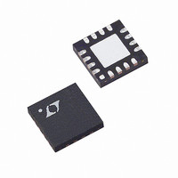
LT6402CUD-6#PBF Linear Technology, LT6402CUD-6#PBF Datasheet

LT6402CUD-6#PBF
Specifications of LT6402CUD-6#PBF
Available stocks
Related parts for LT6402CUD-6#PBF
LT6402CUD-6#PBF Summary of contents
Page 1
... Single Ended to Differential Conversion n Differential to Single Ended Conversion n Level Shifting n IF Sampling Receivers n SAW Filter Interfacing/Buffering L, LT, LTC and LTM are registered trademarks of Linear Technology Corporation. All other trademarks are the property of their respective owners. TYPICAL APPLICATION 5V 0.1μF 0.1μF –INB V CC – ...
Page 2
... Operating Temperature Range (Note 3).... –40°C to 85°C Specifi ed Temperature Range (Note 4) .... –40°C to 85°C Storage Temperature Range ................... –65°C to 125°C Junction Temperature ........................................... 125°C ORDER INFORMATION LEAD FREE FINISH TAPE AND REEL LT6402CUD-6#PBF LT6402CUD-6#TRPBF LT6402IUD-6#PBF LT6402IUD-6#TRPBF LEAD BASED FINISH TAPE AND REEL LT6402CUD-6 ...
Page 3
DC ELECTRICAL CHARACTERISTICS temperature range, otherwise specifi cations are at T shorted to +INB (+IN), –INA shorted to –INB (–IN), V SYMBOL PARAMETER TCV Input Offset Voltage Drift OS I Input Voltage Range, MIN VRMIN I Input Voltage Range, MAX ...
Page 4
LT6402-6 AC ELECTRICAL CHARACTERISTICS ⎯ E ⎯ N ⎯ A ⎯ B ⎯ L ⎯ 0.8V, +INA shorted to +INB (+IN), –INA shorted to –INB (–IN), V unless otherwise noted. SYMBOL PARAMETER Input/Output Characteristics –3dBBW –3dB Bandwidth 0.1dBBW ...
Page 5
AC ELECTRICAL CHARACTERISTICS ⎯ E ⎯ N ⎯ A ⎯ B ⎯ L ⎯ 0.8V, +INA shorted to +INB (+IN), –INA shorted to –INB (–IN), V unless otherwise noted. SYMBOL PARAMETER 25MHz Signal Second/Third Harmonic Distortion Third-Order IMD ...
Page 6
LT6402-6 TYPICAL PERFORMANCE CHARACTERISTICS Third Order Intermodulation Distortion vs Frequency, Differential Input LOAD –45 2 TONES 2V COMPOSITE P-P –55 1MHz TONE SPACING UNFILTERED –65 OUTPUTS –75 FILTERED –85 OUTPUTS –95 –105 ...
Page 7
TYPICAL PERFORMANCE CHARACTERISTICS Noise Figure vs Frequency 40 MEASURED USING DC954 DEMO BOARD 100 1000 FREQUENCY (MHz) 64026 G13 Differential Input Impedance vs Frequency 500 400 300 IMPEDANCE MAGNITUDE 200 100 IMPEDANCE PHASE ...
Page 8
LT6402-6 TYPICAL PERFORMANCE CHARACTERISTICS Overdrive Recovery Time 4.0 +OUT 3.5 3.0 2 100Ω LOAD 2.0 PER OUTPUT 1.5 1.0 –OUT 0.5 0 TIME (25ns/DIV) 64026 G22 Turn-Off Time 4 100Ω PER OUTPUT LOAD 3.5 3.0 +OUT ...
Page 9
PIN FUNCTIONS V (Pin 2): This pin sets the output common mode OCM voltage. Without additional biasing, both inputs bias to this voltage as well. This input is high impedance (Pins 3, 10, 1): Positive ...
Page 10
LT6402-6 BLOCK DIAGRAM –INA 200Ω 14 –INB 200Ω 13 200Ω 200Ω +INA 200Ω 16 +INB 200Ω CCA APPLICATIONS INFORMATION Circuit Description The LT6402 low noise, low distortion differential amplifi er/ADC driver with: • –3dB bandwidth ...
Page 11
APPLICATIONS INFORMATION The LT6402-6 has been designed to minimize the need for external support components such as transformers or AC-coupling capacitors ADC driver, the LT6402-6 requires no external components except for power-supply bypass capacitors. This allows DC-coupled operation ...
Page 12
LT6402-6 APPLICATIONS INFORMATION high impedance inputs of these differential ADCs. If the fi ltered outputs are used, then cutoff frequency and the type of fi lter can be tailored for the specifi c application if needed. Wideband Applications (Using the ...
Page 13
APPLICATIONS INFORMATION can also be used, but since it is being driven differentially it will appear at each fi ltered output as a single-ended capacitance of twice the value. To halve the fi lter band- width, for example, two 42pF ...
Page 14
LT6402-6 APPLICATIONS INFORMATION Large Output Voltage Swings The LT6402-6 has been designed to provide the 3.2V output swing needed by the LTC1748 family of 14-bit low-noise ADCs. This additional output swing improves system SNR 4dB. Input Bias ...
Page 15
... ON THE TOP AND BOTTOM OF PACKAGE Information furnished by Linear Technology Corporation is believed to be accurate and reliable. However, no responsibility is assumed for its use. Linear Technology Corporation makes no representa- tion that the interconnection of its circuits as described herein will not infringe on existing patent rights. UD Package 16-Lead Plastic QFN (3mm × ...
Page 16
... C16 C22 R13 [1] 0.1μF [ 4:1 TEST OUT 4 3 C20, 0.1μ MINI CIRCUITS TCM 4-19 64026 TA02 = 2.6nV/√Hz at 20MHz, 150mW n = 1.9nV/√Hz at 20MHz, 150mW n LT 1007 REV A • PRINTED IN USA © LINEAR TECHNOLOGY CORPORATION 2006 J4 –OUT J5 +OUT 64026fa ...


