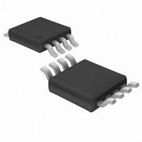
LT1490AHMS8 Linear Technology, LT1490AHMS8 Datasheet

LT1490AHMS8
Specifications of LT1490AHMS8
Available stocks
Related parts for LT1490AHMS8
LT1490AHMS8 Summary of contents
Page 1
... Sensor Conditioning ■ Supply Current Sensing ■ Battery Monitoring Micropower Active Filters ■ ■ 4mA to 20mA Transmitters , LTC and LT are registered trademarks of Linear Technology Corporation. Over-The-Top is a registered trademark of Linear Technology Corporation. Protected by U.S. Patents including 5825228. U TYPICAL APPLICATIO CHARGER VOLTAGE LOAD I ...
Page 2
... OUT – OUT – – MS8 PACKAGE 8-LEAD PLASTIC MSOP = 150°C, θ 250°C/ W JMAX JA MS8 ORDER PART NUMBER PART MARKING LTNG LT1490ACMS8 LTPU LT1490AIMS8 LTRK LT1490AHMS8 TOP VIEW OUT OUT D – – – + + – –IN C OUT OUT C N PACKAGE ...
Page 3
ELECTRICAL CHARACTERISTICS range of – 40°C ≤ T ≤ 85°C, otherwise specifications are otherwise noted. (Note 4) SYMBOL PARAMETER V Input Offset Voltage (Note 5) OS Input Offset Voltage Drift (Note 9) I Input Offset Current OS ...
Page 4
LT1490A/LT1491A ELECTRICAL CHARACTERISTICS range of – 40°C ≤ T ≤ 85°C, otherwise specifications are otherwise noted. (Note 4) SYMBOL PARAMETER PSRR Power Supply Rejection Ratio Minimum Operating Supply Voltage Reverse Supply Voltage I Supply Current per Amplifier ...
Page 5
... T ≤ 70°C A – 40°C ≤ T ≤ 85° ∞ ±10V – ±5V Measure 0°C ≤ T ≤ 70°C A – 40°C ≤ T ≤ 85°C A CONDITIONS LT1490AHS8 LT1490AHMS8, LT1491AHS V = 44V (Note 44V (Note 0. – 0.3V to 44V 3V 500mV to 2.5V 10k 5V 500mV to 4.5V 10k ...
Page 6
... QA sampled at these temperatures. The 6 The ● denotes specifications which apply over the full operating temperature = 0V unless otherwise noted. (Note 4) CM OUT CONDITIONS f = 1kHz = ∞ – LT1490AHS8 LT1490AHMS8, LT1491AHS V = –14.7V to 29V CM = ±14V 10k Load = ±2.5mA I OUT = ±1.25V to ±22V 1kHz = ∞ ...
Page 7
W U TYPICAL PERFOR A CE CHARACTERISTICS Supply Current vs Supply Voltage 125° 25° –55° ...
Page 8
LT1490A/LT1491A W U TYPICAL PERFOR A CE CHARACTERISTICS Gain and Phase Shift vs Frequency 70 = ±2. PHASE GAIN 10 0 –10 –20 – 100 1000 FREQUENCY (kHz) 1490A G10 Gain ...
Page 9
W U TYPICAL PERFOR A CE CHARACTERISTICS Undistorted Output Swing vs Frequency 35 DISTORTION ≤1% = ±15V 5V 0 100 FREQUENCY (kHz) 1490A G19 Total ...
Page 10
LT1490A/LT1491A U U APPLICATIO S I FOR ATIO Supply Voltage The positive supply pin of the LT1490A/LT1491A should be bypassed with a small capacitor (about 0.01µF) within an inch of the pin. When driving heavy loads an additional 4.7µF electrolytic ...
Page 11
U U APPLICATIO S I FOR ATIO Gain The open-loop gain is almost independent of load when the output is sourcing current. This optimizes performance U TYPICAL APPLICATIO S Square Wave Oscillator 59k 5V 100k + 1/2 LT1490A 100k – ...
Page 12
LT1490A/LT1491A PACKAGE DESCRIPTIO 3.5 ±0.05 1.65 ±0.05 2.15 ±0.05 (2 SIDES) 0.25 ± 0.05 0.50 BSC 2.38 ±0.05 (2 SIDES) RECOMMENDED SOLDER PAD PITCH AND DIMENSIONS 5.23 (.206) MIN 0.42 ± 0.04 (.0165 ± .0015) TYP RECOMMENDED SOLDER PAD LAYOUT ...
Page 13
PACKAGE DESCRIPTIO .300 – .325 (7.620 – 8.255) .008 – .015 (0.203 – 0.381) +.035 .325 –.015 ( +0.889 8.255 –0.381 NOTE: 1. DIMENSIONS ARE *THESE DIMENSIONS DO NOT INCLUDE MOLD FLASH OR PROTRUSIONS. MOLD FLASH OR PROTRUSIONS SHALL NOT ...
Page 14
LT1490A/LT1491A PACKAGE DESCRIPTIO .300 – .325 (7.620 – 8.255) .008 – .015 (0.203 – 0.381) +.035 .325 –.015 ( ) +0.889 8.255 –0.381 NOTE: 1. DIMENSIONS ARE MILLIMETERS *THESE DIMENSIONS DO NOT INCLUDE MOLD FLASH OR PROTRUSIONS. MOLD FLASH OR ...
Page 15
... SHADED AREA IS ONLY A REFERENCE FOR PIN 1 LOCATION ON THE TOP AND BOTTOM OF PACKAGE Information furnished by Linear Technology Corporation is believed to be accurate and reliable. However, no responsibility is assumed for its use. Linear Technology Corporation makes no represen- tation that the interconnection of its circuits as described herein will not infringe on existing patent rights. U DHC Package 16-Lead Plastic DFN (5mm × ...
Page 16
... R20 –180V 100k 1490A TA03 , 500V/ 400kHz GBW OS(MAX) VOL(MIN) Extends 44V above MSOP Package, Shutdown Function =55µA (Max), OS(MAX =300µA (Max), OS(MAX) S sn1490, 14901afbs LT/TP 0105 REV B • PRINTED IN USA © LINEAR TECHNOLOGY CORPORATION 2000 R26 2k OPTO1 TEN PHONES ...


