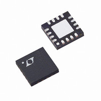
LT6402CUD-20#TRPBF Linear Technology, LT6402CUD-20#TRPBF Datasheet

LT6402CUD-20#TRPBF
Specifications of LT6402CUD-20#TRPBF
Available stocks
Related parts for LT6402CUD-20#TRPBF
LT6402CUD-20#TRPBF Summary of contents
Page 1
... Differential to Single Ended Conversion ■ ■ Level Shifting IF Sampling Receivers ■ SAW Filter Interfacing/Buffering ■ , LT, LTC and LTM are registered trademarks of Linear Technology Corporation. All other trademarks are the property of their respective owners. U TYPICAL APPLICATIO 5V 0.1µF –INB V CC –INA ...
Page 2
... PLASTIC QFN T = 125°C, θ = 68°C/W, θ = 4.2°C/W JMAX JA JC EXPOSED PAD IS V (PIN 17) EE MUST BE SOLDERED TO THE PCB UD PART MARKING* LT6402CUD-20 LCBC LT6402IUD-20 LCBC http://www.linear.com/leadfree/ = 0V, ⎯ E ⎯ N ⎯ A ⎯ B ⎯ L ⎯ 0.8V, +INA = 5V EEA EEB EEC unless otherwise noted. ...
Page 3
DC ELECTRICAL CHARACTERISTICS temperature range, otherwise specifi cations are at T shorted to +INB (+IN), –INA shorted to –INB (–IN), V SYMBOL PARAMETER I Input Voltage Range, MIN VRMIN I Input Voltage Range, MAX VRMAX R Input Resistance INDIFF C ...
Page 4
LT6402-20 AC ELECTRICAL CHARACTERISTICS ⎯ E ⎯ N ⎯ A ⎯ B ⎯ L ⎯ 0.8V, +INA shorted to +INB (+IN), –INA shorted to –INB (–IN), V unless otherwise noted. SYMBOL PARAMETER Input/Output Characteristics –3dBBW –3dB Bandwidth 0.1dBBW ...
Page 5
AC ELECTRICAL CHARACTERISTICS ⎯ E ⎯ N ⎯ A ⎯ B ⎯ L ⎯ 0.8V, +INA shorted to +INB (+IN), –INA shorted to –INB (–IN), V unless otherwise noted. SYMBOL PARAMETER 25MHz Signal Second/Third Harmonic Distortion Third-Order IMD ...
Page 6
LT6402- TYPICAL PERFOR A CE CHARACTERISTICS Third Order Intermodulation Distortion vs Frequency Differential Input LOAD –60 2 TONES, 2V COMPOSITE P-P 1MHz TONE SPACING –65 –70 –75 UNFILTERED OUTPUTS –80 –85 –90 –95 FILTERED OUTPUTS –100 ...
Page 7
W U TYPICAL PERFOR A CE CHARACTERISTICS Noise Figure vs Frequency MEASURED USING DC954A DEMO BOARD 5 10 100 FREQUENCY (MHz) 64022 G15 Differential Input Impedance vs Frequency 400 350 300 250 200 150 IMPEDANCE ...
Page 8
LT6402-20 TYPICAL PERFORMANCE CHARACTERISTICS Large-Signal Transient Response 3 100Ω PER OUTPUT LOAD 3.2 3.0 2.8 2.6 2.4 2.2 2.0 1.8 1.6 1.4 1.2 TIME (10ns/DIV) 64022 G24 Turn-On Time 4 100 LOAD PER OUTPUT 3.5 3.0 ...
Page 9
CTIO S V (Pin 2): This pin sets the output common mode OCM voltage. Without additional biasing, both inputs bias to this voltage as well. This input is high impedance ...
Page 10
LT6402- APPLICATIO S I FOR ATIO Circuit Description The LT6402- low noise, low distortion differential amplifi er/ADC driver with: • –3dB bandwidth DC to 300MHz • Fixed gain independent of R LOAD 10V/V (20dB) • Differential ...
Page 11
U U APPLICATIO S I FOR ATIO Single-Ended to Differential Operation The LT6402-20’s performance with single-ended inputs is comparable to its performance with differential inputs. This excellent single-ended performance is largely due to the internal topology of the LT6402-20. Referring ...
Page 12
LT6402- APPLICATIO S I FOR ATIO Filtered Applications (Using the +OUTFILTERED and –OUTFILTERED Pins) Filtering at the output of the LT6402-20 is often desired to provide either anti-aliasing or improved signal to noise ratio. To simplify this fi ...
Page 13
U U APPLICATIO S I FOR ATIO solution of 14pF from each fi ltered output to ground plus a 14pF capacitor between the fi ltered outputs would also halve the fi lter bandwidth (Figure 7). Bandpass fi ltering is also ...
Page 14
LT6402-20 U TYPICAL APPLICATIO 14 Top Silkscreen 640220fa ...
Page 15
... SHADED AREA IS ONLY A REFERENCE FOR PIN 1 LOCATION ON THE TOP AND BOTTOM OF PACKAGE Information furnished by Linear Technology Corporation is believed to be accurate and reliable. However, no responsibility is assumed for its use. Linear Technology Corporation makes no representation that the interconnection of its circuits as described herein will not infringe on existing patent rights Package 16-Lead Plastic QFN (3mm × ...
Page 16
... TCM 4-19 75Ω R13 C16 C22 [1] 0.1µF [ 4:1 TEST OUT 3 4 C20, 0.1µ MINI CIRCUITS TCM 4-19 6402 TA02 = 3.8nV/√Hz at 20MHz, 150mV n = 2.6nV/√Hz at 20MHz, 150mV n LT 0706 • PRINTED IN USA © LINEAR TECHNOLOGY CORPORATION 2005 J4 –OUT J5 +OUT 640220fa ...


