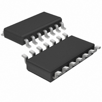
LT1491CS#TRPBF Linear Technology, LT1491CS#TRPBF Datasheet - Page 4

LT1491CS#TRPBF
Manufacturer Part Number
LT1491CS#TRPBF
Description
IC OP-AMP R-R IN/OUT QUAD 14SOIC
Manufacturer
Linear Technology
Series
Over-The-Top®r
Datasheet
1.LT1490CN8PBF.pdf
(12 pages)
Specifications of LT1491CS#TRPBF
Amplifier Type
General Purpose
Number Of Circuits
4
Output Type
Rail-to-Rail
Slew Rate
0.07 V/µs
Gain Bandwidth Product
200kHz
Current - Input Bias
1nA
Voltage - Input Offset
400µV
Current - Supply
50µA
Current - Output / Channel
25mA
Voltage - Supply, Single/dual (±)
2 V ~ 44 V, ±1 V ~ 22 V
Operating Temperature
0°C ~ 70°C
Mounting Type
Surface Mount
Package / Case
14-SOIC (3.9mm Width), 14-SOL
Lead Free Status / RoHS Status
Lead free / RoHS Compliant
-3db Bandwidth
-
Available stocks
Company
Part Number
Manufacturer
Quantity
Price
LT1490/LT1491
ELECTRICAL CHARACTERISTICS
range, otherwise specifications are at T
SYMBOL
V
V
I
I
e
i
R
C
CMRR
A
V
I
PSRR
I
GBW
SR
Note 1: Absolute Maximum Ratings are those values beyond which the
life of the device may be impaired.
Note 2: A heat sink may be required to keep the junction temperature
below absolute maximum. This depends on the power supply voltage
and how many amplifiers are shorted.
Note 3: The LT1490C/LT1491C are guaranteed to meet specified
performance from 0 C to 70 C. The LT1490C/LT1491C are designed,
characterized and expected to meet specified performance from – 40 C
to 85 C but are not tested or QA sampled at these temperatures.
4
n
OS
B
SC
S
n
OS
OS
IN
VOL
O
IN
TC
PARAMETER
Input Offset Voltage
Input Offset Voltage Drift
Input Offset Current
Input Bias Current
Input Noise Voltage
Input Noise Voltage Density
Input Noise Current Density
Input Resistance
Input Capacitance
Input Voltage Range
Common Mode Rejection Ratio
Large-Signal Voltage Gain
Output Voltage Swing
Short-Circuit Current (Note 2)
Power Supply Rejection Ratio
Supply Current per Amplifier
Gain Bandwidth Product
Slew Rate
A
= 25 C. V
CONDITIONS
0 C T
– 40 C T
LT1491 N Package
0 C T
– 40 C T
LT1490CMS8 Package, LT1491 S Package
0 C T
– 40 C T
0 C T
– 40 C T
0.1Hz to 10Hz
f = 1kHz
f = 1kHz
Differential
Common Mode, V
V
V
0 C T
– 40 C T
No Load
I
I
Short to GND
0 C T
– 40 C T
V
0 C T
– 40 C T
A
Measure at V
0 C T
– 40 C T
LT1490 N, S Package
f = 1kHz
OUT
OUT
CM
O
S
V
= 1.25V to 22V
= – 1, R
= 14V, R
= – 15V to 29V
= 5mA
= 10mA
S
A
A
A
A
A
A
A
A
= 15V, V
A
A
A
A
A
A
A
L
A
70 C
70 C
70 C
70 C (Note 7)
70 C
70 C
70 C
70 C
The
=
O
L
85 C
85 C
85 C
85 C (Note 7)
85 C
85 C
85 C
85 C
= 5V
= 10k
V
CM
O
CM
denotes specifications which apply over the full operating temperature
= 10V,
= – 15V to 14V
= 0V, V
The LT1490I/LT1491I are guaranteed to meet specified performance from
– 40 C to 85 C.
Note 4: V
V
Note 5: V
V
Note 6: Guaranteed by correlation to slew rate at V
at V
Note 7: This parameter is not 100% tested.
S
S
= 15V tests.
= 15V tests.
OUT
S
= 3V and V
= 0V, unless otherwise noted. (Note 3)
S
S
= 5V limits are guaranteed by correlation to V
= 3V limits are guaranteed by correlation to V
S
= 15V tests.
0.0375
0.0330
0.0300
MIN
– 15
100
125
110
100
14.9
14.5
14.5
80
75
50
88
6
20
15
10
15000
14.978
14.750
14.670
0.03
0.07
TYP
250
350
400
250
200
0.2
4.6
50
17
98
98
50
3
3
4
1
25
S
= 15V and GBW
MAX
1200
1400
1500
1250
1500
1600
1600
1850
1950
0.8
29
70
85
6
6
8
S
S
= 3V and
= 5V and
nV/ Hz
pA/ Hz
UNITS
V/mV
V/mV
V/mV
V/ C
V/ C
V/ s
V/ s
V/ s
V
M
M
kHz
kHz
kHz
mA
mA
mA
P-P
nA
nA
dB
dB
pF
V
V
V
V
V
V
V
V
V
V
V
V
V
A
A


