LT1364CN8 Linear Technology, LT1364CN8 Datasheet
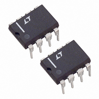
IC OP-AMP HI-SPD 70MHZ DUAL 8DIP

LT1364CN8

Manufacturer Part Number
LT1364CN8
Description
IC OP-AMP HI-SPD 70MHZ DUAL 8DIP
Manufacturer
Linear Technology
Series
C-Load™r
Datasheet

Specifications of LT1364CN8

Amplifier Type
Voltage Feedback
Number Of Circuits
2
Slew Rate
1000 V/µs
Gain Bandwidth Product
70MHz
Current - Input Bias
600nA
Voltage - Input Offset
500µV
Current - Supply
6.3mA
Current - Output / Channel
60mA
Voltage - Supply, Single/dual (±)
5 V ~ 36 V, ±2.5 V ~ 18 V
Operating Temperature
0°C ~ 70°C
Mounting Type
Through Hole
Package / Case
8-DIP (0.300", 7.62mm)
Lead Free Status / RoHS Status
Contains lead / RoHS non-compliant
Output Type
-
-3db Bandwidth
-

Available stocks

Company
Part Number
Manufacturer
Quantity
Price
Part Number:
LT1364CN8
Manufacturer:
LT
Quantity:
5 510
Part Number:
LT1364CN8
Manufacturer:
LT
Quantity:
1 000
Part Number:
LT1364CN8
Manufacturer:
LT/凌特
Quantity:
20 000
Part Number:
LT1364CN8#PBF
Manufacturer:
JOHANSON
Quantity:
460 000
Part Number:
LT1364CN8#PBF
Manufacturer:
LINEAR/凌特
Quantity:
20 000
FEATURES
APPLICATIO S
TYPICAL APPLICATIO
70MHz Gain Bandwidth
1000V/ s Slew Rate
7.5mA Maximum Supply Current per Amplifier
Unity-Gain Stable
C-Load
9nV/ Hz Input Noise Voltage
1.5mV Maximum Input Offset Voltage
2 A Maximum Input Bias Current
350nA Maximum Input Offset Current
50mA Minimum Output Current
4.5V/mV Minimum DC Gain, R
50ns Settling Time to 0.1%, 10V Step
0.06% Differential Gain, A
0.04 Differential Phase, A
Specified at 2.5V, 5V, and 15V
Wideband Amplifiers
Buffers
Active Filters
Video and RF Amplification
Cable Drivers
Data Acquisition Systems
7.5V Minimum Output Swing into 150
TM
–4
–6
–2
–8
Op Amp Drives All Capacitive Loads
2
0
1
Cable Driver Frequency Response
IN
510
LT1364
+
1/2
U
510
FREQUENCY (MHz)
V
S
= 2.5V
75
V
S
V
= 5V
10
S
V
V
= 10V
=2, R
=2, R
75
OUT
L
U
=1k
L
L
V
=150
=150
S
1364/1365 TA01
= 15V
100
DESCRIPTIO
The LT1364/LT1365 are dual and quad high speed opera-
tional amplifiers with outstanding AC and DC perfor-
mance. The amplifiers feature much lower supply current
and higher slew rate than devices with comparable band-
width. The circuit topology is a voltage feedback amplifier
with matched high impedance inputs and the slewing
performance of a current feedback amplifier. The high
slew rate and single stage design provide excellent settling
characteristics which make the circuit an ideal choice for
data acquisition systems. Each output drives a 150 load
to 7.5V with 15V supplies and to 3.4V on 5V sup-
plies. The amplifiers are stable with any capacitive load
making them useful in buffer or cable driving applications.
The LT1364/LT1365 are members of a family of fast, high
performance amplifiers using this unique topology and
employing Linear Technology Corporation’s advanced
bipolar complementary processing. For a single amplifier
version of the LT1364/LT1365 see the LT1363 data sheet.
For 50MHz devices with 4mA supply currents see the
LT1360 through LT1362 data sheets. For lower supply
current amplifiers see the LT1354 to LT1359 data sheets.
Singles, duals, and quads of each amplifier are available.
C-Load is a trademark of Linear Technology Corporation
, LTC and LT are registered trademarks of Linear Technology Corporation.
70MHz, 1000V/ s Op Amps
A
V
= –1 Large-Signal Response
U
Dual and Quad
LT1364/LT1365
1364/1365 TA02
1

Related parts for LT1364CN8

LT1364CN8 Summary of contents

Page 1

... For 50MHz devices with 4mA supply currents see the LT1360 through LT1362 data sheets. For lower supply current amplifiers see the LT1354 to LT1359 data sheets. Singles, duals, and quads of each amplifier are available. , LTC and LT are registered trademarks of Linear Technology Corporation. C-Load is a trademark of Linear Technology Corporation V = 15V ...

Page 2

... Specified Temperature Range (Note 9) ....– Maximum Junction Temperature (See Below) Plastic Package ................................................ 150 C S Storage Temperature Range ..................– 150 C Lead Temperature (Soldering, 10 sec).................. 300 ORDER PART NUMBER OUT A 1 – LT1364CN8 + – 8-LEAD PLASTIC 150 C, JMAX ORDER PART NUMBER OUT A 1 –IN A ...

Page 3

ELECTRICAL CHARACTERISTICS SYMBOL PARAMETER + Input Voltage Range – Input Voltage Range CMRR Common Mode Rejection Ratio PSRR Power Supply Rejection Ratio A Large-Signal Voltage Gain VOL V Output Swing OUT I Output Current OUT I Short-Circuit Current SC SR ...

Page 4

LT1364/LT1365 ELECTRICAL CHARACTERISTICS unless otherwise noted SYMBOL PARAMETER V Input Offset Voltage OS Input V Drift OS I Input Offset Current OS I Input Bias Current B CMRR Common Mode ...

Page 5

ELECTRICAL CHARACTERISTICS – unless otherwise noted. (Note SYMBOL PARAMETER V Output Swing OUT I Output Current OUT I Short-Circuit Current SC SR Slew Rate GBW Gain Bandwidth Channel Separation ...

Page 6

LT1364/LT1365 W U TYPICAL PERFORMANCE CHARACTERISTICS Input Bias Current vs Temperature 1 15V – 1 ———— 1.0 0.8 0.6 0.4 0.2 0 –50 – ...

Page 7

W U TYPICAL PERFORMANCE CHARACTERISTICS Output Impedance vs Frequency 100 V = 15V 100 0.1 0.01 10k 100k 1M 10M 100M ...

Page 8

LT1364/LT1365 W U TYPICAL PERFORMANCE CHARACTERISTICS Slew Rate vs Supply Voltage 2400 2200 A = –1 V 2000 – 1800 SR = ————— 1600 ...

Page 9

W U TYPICAL PERFORMANCE CHARACTERISTICS Small-Signal Transient ( 1364/1365 TA31 Large-Signal Transient ( 1364/1365 TA34 U U APPLICATIONS INFORMATION Layout and Passive Components The LT1364/LT1365 amplifiers are easy to use and toler- ant of ...

Page 10

... Because of the wide supply voltage range possible to exceed the maximum junction temperature under certain conditions. Maximum junction temperature (T temperature (T LT1364CN8: T LT1364CS8: T LT1365CN: T LT1365CS: T Worst case power dissipation occurs at the maximum supply current and when the output voltage is at 1/2 of either supply voltage (or the maximum swing if less than 1/2 supply voltage) ...

Page 11

... MOLD FLASH OR PROTRUSIONS SHALL NOT EXCEED 0.010 INCH (0.254mm) Information furnished by Linear Technology Corporation is believed to be accurate and reliable. However, no responsibility is assumed for its use. Linear Technology Corporation makes no represen- tation that the interconnection of its circuits as described herein will not infringe on existing patent rights. ...

Page 12

... SO8 1298 0.386 – 0.394* (9.804 – 10.008 1mV, 4mA/Amplifier OS = 0.6mV, 2mA/Amplifier OS 13645fa LT/TP 0400 2K REV A • PRINTED IN USA LINEAR TECHNOLOGY CORPORATION 1994 V OUT 1364/1365 TA04 0.150 – 0.157** (3.810 – 3.988) S16 1098 ...

Related keywords