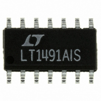
LT1491AIS Linear Technology, LT1491AIS Datasheet - Page 10

LT1491AIS
Manufacturer Part Number
LT1491AIS
Description
IC OP-AMP R-R IN/OUT QUAD 14SOIC
Manufacturer
Linear Technology
Series
Over-The-Top®r
Datasheet
1.LT1490ACN8.pdf
(16 pages)
Specifications of LT1491AIS
Amplifier Type
General Purpose
Number Of Circuits
4
Output Type
Rail-to-Rail
Slew Rate
0.07 V/µs
Gain Bandwidth Product
200kHz
Current - Input Bias
1nA
Voltage - Input Offset
250µV
Current - Supply
50µA
Current - Output / Channel
25mA
Voltage - Supply, Single/dual (±)
2 V ~ 44 V, ±1 V ~ 22 V
Operating Temperature
-40°C ~ 85°C
Mounting Type
Surface Mount
Package / Case
14-SOIC (3.9mm Width), 14-SOL
Lead Free Status / RoHS Status
Contains lead / RoHS non-compliant
-3db Bandwidth
-
Other names
Q1477605
Available stocks
Company
Part Number
Manufacturer
Quantity
Price
Part Number:
LT1491AIS
Manufacturer:
LINEAR/凌特
Quantity:
20 000
Company:
Part Number:
LT1491AIS#PBF
Manufacturer:
ADI
Quantity:
2 995
Part Number:
LT1491AIS#PBF
Manufacturer:
LINEAR/凌特
Quantity:
20 000
Part Number:
LT1491AIS#TRPBF
Manufacturer:
ADI/亚德诺
Quantity:
20 000
APPLICATIO S I FOR ATIO
LT1490A/LT1491A
Supply Voltage
The positive supply pin of the LT1490A/LT1491A should
be bypassed with a small capacitor (about 0.01µF) within
an inch of the pin. When driving heavy loads an additional
4.7µF electrolytic capacitor should be used. When using
split supplies, the same is true for the negative supply pin.
The LT1490A/LT1491A are protected against reverse bat-
tery voltages up to 18V. In the event a reverse battery
condition occurs, the supply current is less than 1nA.
The LT1490A/LT1491A can be shut down by removing V
In this condition the input bias current is typically less than
0.5nA, even if the inputs are 44V above the negative
supply.
When operating the LT1490A/LT1491A on total supplies
of 20V or more, the supply must not rise to its final voltage
in less than 1µs. This is especially true if low ESR bypass
capacitors are used. A series RLC circuit is formed from
the supply lead inductance and the bypass capacitor. A
resistance of 7.5Ω in the supply or in the bypass capacitor
will dampen the tuned circuit enough to limit the rise time.
Inputs
The LT1490A/LT1491A have two input stages, NPN and
PNP (see the Simplified Schematic), resulting in three
distinct operating regions as shown in the Input Bias
Current vs Common Mode typical performance curve.
For input voltages about 0.8V or more below V
input stage is active and the input bias current is typically
– 1nA. When the input voltage is about 0.5V or less from
V
current is typically 25nA. Increases in temperature will
cause the voltage at which operation switches from the
PNP stage to the NPN stage to move towards V
offset voltage of the NPN stage is untrimmed and is
typically 600µV.
A Schottky diode in the collector of each NPN transistor of
the NPN input stage allows the LT1490A/LT1491A to op-
erate with either or both of their inputs above V
0.3V above V
and the input bias current is typically 3µA at room tem-
perature. The input offset voltage is typically 700µV when
10
+
, the NPN input stage is operating and the input bias
+
the NPN input transistor is fully saturated
U
U
W
+
+
U
+
. The input
. At about
, the PNP
+
.
operating above V
with their inputs 44V above V
The inputs are protected against excursions as much as
15V below V
each input and a diode from the input to the negative
supply. There is no output phase reversal for inputs up to
15V below V
inputs and the maximum differential input voltage is 44V.
Output
The output voltage swing of the LT1490A/LT1491A is
affected by input overdrive as shown in the typical perfor-
mance curves.
The output of the LT1490A/LT1491A can be pulled up to
18V beyond V
provided that V
The normally reverse-biased substrate diode from the
output to V
output is forced below V
limited to 100mA, no damage will occur.
The LT1490A/LT1491A are internally compensated to
drive at least 200pF of capacitance under any output
loading conditions. A 0.22µF capacitor in series with a
150Ω resistor between the output and ground will com-
pensate these amplifiers for larger capacitive loads, up to
10,000pF, at all output currents.
Distortion
There are two main contributors of distortion in op amps:
output crossover distortion as the output transitions
from sourcing to sinking current and distortion caused
by nonlinear common mode rejection. Of course, if the op
amp is operating inverting there is no common mode
induced distortion. When the LT1490A/LT1491A switch
between input stages there is significant nonlinearity in
the CMRR. Lower load resistance increases the output
crossover distortion, but has no effect on the input stage
transition distortion. For lowest distortion the LT1490A/
LT1491A should be operated single supply, with the
output always sourcing current and with the input volt-
age swing between ground and (V
Typical Performance Characteristics curves.
–
will cause unlimited currents to flow when the
–
–
. There are no clamping diodes between the
+
by an internal 1k resistor in series with
+
with less than 1nA of leakage current,
is less than 0.5V.
+
. The LT1490A/LT1491A will operate
–
. If the current is transient and
–
regardless of V
+
– 0.8V). See the
sn1490, 14901afbs
+
.


