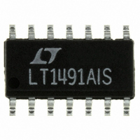
LT1491AIS Linear Technology, LT1491AIS Datasheet - Page 6

LT1491AIS
Manufacturer Part Number
LT1491AIS
Description
IC OP-AMP R-R IN/OUT QUAD 14SOIC
Manufacturer
Linear Technology
Series
Over-The-Top®r
Datasheet
1.LT1490ACN8.pdf
(16 pages)
Specifications of LT1491AIS
Amplifier Type
General Purpose
Number Of Circuits
4
Output Type
Rail-to-Rail
Slew Rate
0.07 V/µs
Gain Bandwidth Product
200kHz
Current - Input Bias
1nA
Voltage - Input Offset
250µV
Current - Supply
50µA
Current - Output / Channel
25mA
Voltage - Supply, Single/dual (±)
2 V ~ 44 V, ±1 V ~ 22 V
Operating Temperature
-40°C ~ 85°C
Mounting Type
Surface Mount
Package / Case
14-SOIC (3.9mm Width), 14-SOL
Lead Free Status / RoHS Status
Contains lead / RoHS non-compliant
-3db Bandwidth
-
Other names
Q1477605
Available stocks
Company
Part Number
Manufacturer
Quantity
Price
Part Number:
LT1491AIS
Manufacturer:
LINEAR/凌特
Quantity:
20 000
Company:
Part Number:
LT1491AIS#PBF
Manufacturer:
ADI
Quantity:
2 995
Part Number:
LT1491AIS#PBF
Manufacturer:
LINEAR/凌特
Quantity:
20 000
Part Number:
LT1491AIS#TRPBF
Manufacturer:
ADI/亚德诺
Quantity:
20 000
LT1490A/LT1491A
ELECTRICAL CHARACTERISTICS
range of – 40°C ≤ T
SYMBOL
I
GBW
SR
V
I
I
CMRR
A
V
PSRR
I
GBW
SR
Note 1: Absolute Maximum Ratings are those values beyond which the life
of the device may be impaired.
Note 2: A heat sink may be required to keep the junction temperature
below absolute maximum. This depends on the power supply voltage and
how many amplifiers are shorted. The θ
package is with minimal PCB heat spreading metal. Using expanded metal
area on all layers of a board reduces this value.
Note 3: The LT1490AC/LT1491AC and LT1490AI/LT1491AI are guaranteed
functional over the operating temperature range of – 40°C to 85°C. The
LT1490AH/LT1491AH are guaranteed functional over the operating
temperature range of – 40°C to 125°C.
Note 4: The LT1490AC/LT1491AC are guaranteed to meet specified
performance from 0°C to 70°C. The LT1490AC/LT1491AC are designed,
characterized and expected to meet specified performance from – 40°C to
85°C but are not tested or QA sampled at these temperatures. The
6
S
OS
B
S
OS
VOL
O
PARAMETER
Supply Current per Amplifier (Note 7)
Gain Bandwidth Product (Note 6)
Slew Rate (Note 8)
Input Offset Voltage (Note 5)
Input Offset Voltage Drift (Note 9)
Input Offset Current
Input Bias Current
Input Voltage Range
Common Mode Rejection Ratio
Large-Signal Voltage Gain
Output Voltage Swing
Power Supply Rejection Ratio
Supply Current per Amplifier
Gain Bandwidth Product
Slew Rate
A
≤ 125°C. V
S
= ±15V, V
JA
specified for the DD and DHC
CM
CONDITIONS
A
LT1490AHMS8, LT1491AHS
V
V
No Load
I
V
A
f = 1kHz
LT1490AHS8
f = 1kHz
= 0V, V
OUT
V
CM
O
S
V
= – 1, R
= ±1.25V to ±22V
= – 1, R
= ±14V, R
= –14.7V to 29V
= ±2.5mA
OUT
L
L
The
= ∞
= ∞
L
= 0V unless otherwise noted. (Note 4)
= 10k
●
denotes specifications which apply over the full operating temperature
LT1490AI/LT1491AI are guaranteed to meet specified performance from
–40°C to 85°C. The LT1490AH/LT1491AH are guaranteed to meet
specified performance from – 40°C to 125°C.
Note 5: ESD (Electrostatic Discharge) sensitive device. Extensive use of
ESD protection devices are used internal to the LT1490A/LT1491A.
However, high electrostatic discharge can damage or degrade the device.
Use proper ESD handling precautions.
Note 6: V
V
Note 7: V
V
Note 8: Guaranteed by correlation to slew rate at V
at V
Note 9: This parameter is not 100% tested.
S
S
= ±15V tests.
= ±15V tests.
S
= 3V and V
S
S
= 5V limits are guaranteed by correlation to V
= 3V limits are guaranteed by correlation to V
S
= ±15V tests.
●
●
●
●
●
●
●
●
●
●
●
●
●
●
●
●
●
0.0375
–14.7
0.035
0.015
±14.8
±14.3
0.02
MIN
110
100
125
60
72
84
75
4
LT1490AH/LT1491AH
0.06
0.07
TYP
180
150
250
250
200
40
50
3
S
= ±15V and GBW
MAX
2700
1200
3200
700
50
70
20
29
70
95
7
2
S
S
= 3V and
sn1490, 14901afbs
= 5V and
UNITS
µV/°C
V/mV
V/mV
V/µs
V/µs
V/µs
V/µs
kHz
kHz
kHz
kHz
mV
mV
µA
µA
µA
µV
µV
µV
µV
nA
nA
dB
dB
µA
V


