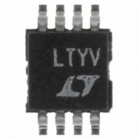
LTC1992-2CMS8 Linear Technology, LTC1992-2CMS8 Datasheet - Page 24

LTC1992-2CMS8
Manufacturer Part Number
LTC1992-2CMS8
Description
IC AMP/DVR I/O GAIN OF 2 8MSOP
Manufacturer
Linear Technology
Datasheet
1.LTC1992CMS8PBF.pdf
(42 pages)
Specifications of LTC1992-2CMS8
Amplifier Type
Differential
Number Of Circuits
1
Output Type
Differential, Rail-to-Rail
Slew Rate
1.5 V/µs
Gain Bandwidth Product
3.2MHz
Current - Input Bias
2pA
Voltage - Input Offset
250µV
Current - Supply
700µA
Current - Output / Channel
30mA
Voltage - Supply, Single/dual (±)
2.7 V ~ 11 V, ±1.35 V ~ 5.5 V
Operating Temperature
0°C ~ 70°C
Mounting Type
Surface Mount
Package / Case
8-MSOP, Micro8™, 8-uMAX, 8-uSOP,
Lead Free Status / RoHS Status
Contains lead / RoHS non-compliant
-3db Bandwidth
-
Available stocks
Company
Part Number
Manufacturer
Quantity
Price
Company:
Part Number:
LTC1992-2CMS8
Manufacturer:
LT
Quantity:
10 000
Part Number:
LTC1992-2CMS8
Manufacturer:
LINEAR/凌特
Quantity:
20 000
Company:
Part Number:
LTC1992-2CMS8#PBF
Manufacturer:
LT
Quantity:
759
pin FuncTions
LTC1992 Family
–IN, +IN (Pins 1, 8): Inverting and Noninverting Inputs
of the Amplifier. For the LTC1992 part, these pins are
connected directly to the amplifier’s P-channel MOSFET
input devices. The fixed gain LTC1992-X parts have preci-
sion, on-chip gain setting resistors. The input resistors
are nominally 30k for the LTC1992-1, LTC1992-2 and
LTC1992-5 parts. The input resistors are nominally 15k
for the LTC1992-10 part.
V
The voltage on this pin sets the output signal’s common
mode voltage level. The output common mode level is set
independent of the input common mode level. This is a
high impedance input and must be connected to a known
and controlled voltage. It must never be left floating.
block DiagraMs
OCM
(Pin 2): Output Common Mode Voltage Set Pin.
V
V
OCM
MID
–IN
+IN
1
7
2
8
(1992)
V
V
+
–
200k
200k
+V
–V
+V
–V
S
S
S
S
–
+
A1
–
+
+
+
+V
–V
+V
should be bypassed with 0.1µF capacitors to an adequate ana-
log ground or ground plane. The bypass capacitors should
be located as closely as possible to the supply pins.
+OUT, –OUT (Pins 4, 5): The Positive and Negative
Outputs of the Amplifier. These rail-to-rail outputs are
designed to drive capacitive loads as high as 10,000pF .
V
to an on-chip resistive voltage divider to provide a mid-
supply reference. This provides a convenient way to set
the output common mode level at half-supply. If used for
this purpose, Pin 2 will be shorted to Pin 7, Pin 7 should
be bypassed with a 0.1µF capacitor to ground. If this refer-
ence voltage is not used, leave the pin floating.
3
6
S
S
MID
S
, –V
A2
(Pin 7): Mid-Supply Reference. This pin is connected
–
+
S
(Pins 3, 6): The +V
30k
30k
1992 BD
4
5
+OUT
–OUT
S
and –V
S
power supply pins
1992fa


