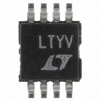
LTC1992-2CMS8 Linear Technology, LTC1992-2CMS8 Datasheet - Page 36

LTC1992-2CMS8
Manufacturer Part Number
LTC1992-2CMS8
Description
IC AMP/DVR I/O GAIN OF 2 8MSOP
Manufacturer
Linear Technology
Datasheet
1.LTC1992CMS8PBF.pdf
(42 pages)
Specifications of LTC1992-2CMS8
Amplifier Type
Differential
Number Of Circuits
1
Output Type
Differential, Rail-to-Rail
Slew Rate
1.5 V/µs
Gain Bandwidth Product
3.2MHz
Current - Input Bias
2pA
Voltage - Input Offset
250µV
Current - Supply
700µA
Current - Output / Channel
30mA
Voltage - Supply, Single/dual (±)
2.7 V ~ 11 V, ±1.35 V ~ 5.5 V
Operating Temperature
0°C ~ 70°C
Mounting Type
Surface Mount
Package / Case
8-MSOP, Micro8™, 8-uMAX, 8-uSOP,
Lead Free Status / RoHS Status
Contains lead / RoHS non-compliant
-3db Bandwidth
-
Available stocks
Company
Part Number
Manufacturer
Quantity
Price
Company:
Part Number:
LTC1992-2CMS8
Manufacturer:
LT
Quantity:
10 000
Part Number:
LTC1992-2CMS8
Manufacturer:
LINEAR/凌特
Quantity:
20 000
Company:
Part Number:
LTC1992-2CMS8#PBF
Manufacturer:
LT
Quantity:
759
LTC1992 Family
applicaTions inForMaTion
quantifies the undesired effect of signal level shifting
discussed earlier in the Signal Level Shifting section.
Asymmetrical Feedback Application Circuits
The basic signal equation in Figure 6 also gives insight
to another piece of intuition. The feedback factors may
be deliberately set to different values. One interesting
class of these application circuits sets one or both of the
feedback factors to the extreme values of either zero or
one. Figure 7 shows three such circuits.
At first these application circuits may look to be unstable
or open loop. It is the common mode feedback loop that
enables these circuits to function. While they are useful
circuits, they have some shortcomings that must be con-
sidered. First, do to the severe feedback factor asymmetry,
the V
with about the same strength as the input signal. With
this much gain in the V
and noise increase. The large V
necessitates that these circuits are largely limited to dual,
OCM
level influences the differential output voltage
Figure 6. Basic Equations for Mismatched or Asymmetrical Feedback Applications Circuits
OCM
WHERE:
• FOR GROUND REFERENCED, SINGLE-ENDED INPUT SIGNAL, LET +V
• COMMON MODE REJECTION: SET +V
• OUTPUT DC OFFSET VOLTAGE: SET +V
+V
path, differential output offset
IN
V
– –V
INDIFF
V
V
CMRR =
V
OCM
OUTDIFF
1 =
OUTDIFF
OSDIFFOUT
IN
R
IN1
to V
–V
+V
R
=
=
∆V
2[+V
IN1
+ R
∆V
IN
IN
2 • V
= V
OUTDIFF
INCM
FB1
OUTDIFF
OSDIFF
IN
INSIG
; 2 =
R
R
• (1 – 1) – (–V
IN2
IN1
= 2
• (1 – 1) + 2V
V
R
1 + 2
OCM
IN2
1 + 2
2 – 1
2
gain also
R
IN2
+ R
IN
IN
+ (V
= –V
FB2
; OUTPUT REFERRED
= –V
IN
OUTCM
) • (1 – 2)] + 2V
1 + 2
V
–
+
OSDIFF
IN
OCM
IN
; V
R
R
= V
V
0.999 < K
= V
FB2
FB1
OSDIFF
OUTCM
+
–
INCM
– V
1 + 2
INCM
+ 2V
LTC1992
INCM
, V
split supply voltage applications with a ground referenced
input signal and a grounded V
The top application circuit in Figure 7 yields a high input
impedance, precision gain of 2 block without any external
resistors. The on-chip common mode feedback servo
resistors determine the gain precision (better than 0.1
percent). By using the –V
also useful to get a precision, single-ended output, high
input impedance inverter. To intuitively understand this
circuit, consider it as a standard op amp voltage follower
(delivered through the signal gain servo) with a comple-
mentary output (delivered through the common mode level
servo). As usual, the amplifier’s input common mode range
must not be exceeded. As with a standard op amp voltage
follower, the common mode signal seen at the amplifier’s
input is the input signal itself. This condition limits the
input signal swing, as well as the output signal swing, to
be the input signal common mode range specification.
The middle circuit is largely the same as the first except
that the noninverting amplifier path has gain. Note that
OUTCM
= AMPLIFIER INPUT REFERRED OFFSET VOLTAGE
= K
CM
OSDIFF
) 2
CM
OSDIFF
< 1.001
2 – 1
1 + 2
• V
( 1 – 2)
= 0V, V
OCM
+ 2V
IN
+V
–V
+ V
= V
OUTCM
OUT
OUT
OUTCM
OSCM
INSIG
V
+V
= 0V
( 1 – 2)
OUTDIFF
AND –V
OUT
– –V
IN
1992 F06
OUT
= 0V
OUT
output alone, this circuit is
OCM
pin.
1992fa


