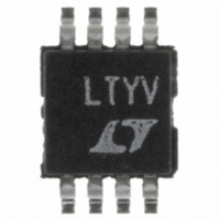
LTC1992-2CMS8 Linear Technology, LTC1992-2CMS8 Datasheet - Page 5

LTC1992-2CMS8
Manufacturer Part Number
LTC1992-2CMS8
Description
IC AMP/DVR I/O GAIN OF 2 8MSOP
Manufacturer
Linear Technology
Datasheet
1.LTC1992CMS8PBF.pdf
(42 pages)
Specifications of LTC1992-2CMS8
Amplifier Type
Differential
Number Of Circuits
1
Output Type
Differential, Rail-to-Rail
Slew Rate
1.5 V/µs
Gain Bandwidth Product
3.2MHz
Current - Input Bias
2pA
Voltage - Input Offset
250µV
Current - Supply
700µA
Current - Output / Channel
30mA
Voltage - Supply, Single/dual (±)
2.7 V ~ 11 V, ±1.35 V ~ 5.5 V
Operating Temperature
0°C ~ 70°C
Mounting Type
Surface Mount
Package / Case
8-MSOP, Micro8™, 8-uMAX, 8-uSOP,
Lead Free Status / RoHS Status
Contains lead / RoHS non-compliant
-3db Bandwidth
-
Available stocks
Company
Part Number
Manufacturer
Quantity
Price
Company:
Part Number:
LTC1992-2CMS8
Manufacturer:
LT
Quantity:
10 000
Part Number:
LTC1992-2CMS8
Manufacturer:
LINEAR/凌特
Quantity:
20 000
Company:
Part Number:
LTC1992-2CMS8#PBF
Manufacturer:
LT
Quantity:
759
elecTrical characTerisTics
temperature range, otherwise specifications are at T
noted. V
defined as (+V
LTC1992-1 only.
SYMBOL PARAMETER
G
e
R
V
CMRR
SR
GBW
The
+V
as (+V
Typical values are at T
SYMBOL PARAMETER
G
e
R
V
CMRR
SR
GBW
n
n
INCMR
INCMR
DIFF
IN
DIFF
IN
S
l
= 5V, –V
OUT
denotes the specifications which apply over the full operating temperature range, otherwise specifications are at T
OCM
Differential Gain
Differential Gain Error
Differential Gain Nonlinearity
Differential Gain Temperature Coefficient
Input Referred Noise Voltage Density (Note 7) f = 1kHz
Input Resistance, Single-Ended +IN, –IN Pins
Input Signal Common Mode Range
Common Mode Rejection Ratio
(Amplifier Input Referred) (Note 7)
Slew Rate (Note 4)
Gain-Bandwidth Product
+ –V
S
is the voltage on the V
= 0V, V
IN
OUT
– –V
)/2. V
INCM
IN
A
). V
INCM
= 25°C. Specifications apply to the LTC1992-2 only.
= V
OUTDIFF
is defined as (+V
OUTCM
is defined as (+V
OCM
= V
OCM
pin. V
= 2.5V, unless otherwise noted. V
OUTCM
IN
+ –V
CONDITIONS
V
V
f
CONDITIONS
V
V
f
OUT
TEST
TEST
S
INCM
S
INCM
is defined as (+V
IN
A
= 5V
= 5V
)/2. V
= 25°C. +V
– –V
= 180kHz
= 180kHz
= –0.1V to 3.7V
= –0.1V to 3.7V
The
OUT
INDIFF
). Typical values are at T
l
S
denotes the specifications which apply over the full operating
is defined as (+V
= 5V, –V
OUT
l
l
l
l
l
l
l
l
l
l
+ –V
S
= 0V, V
22.5
OCM
22.5
MIN
MIN
OUT
0.5
0.7
55
55
LTC1992-1CMS8
LTC1992-2CMS8
LTC1992-1ISM8
LTC1992-2ISM8
)/2. V
is the voltage on the V
–0.1V to 4.9V
–0.1V to 4.9V
IN
INCM
– –V
±0.1
±0.1
TYP
TYP
INCM
3.5
1.5
3.5
50
45
30
60
50
45
30
60
1
3
2
2
4
A
= V
= 25°C. Specifications apply to the
IN
). V
is defined as (+V
OUTCM
MAX
MAX
±0.3
37.5
OUTDIFF
±0.3
37.5
= V
LTC1992 Family
OCM
is defined as (+V
MIN
OCM
MIN
0.5
0.7
22
55
22
55
= 2.5V, unless otherwise
LTC1992-1HMS8
LTC1992-2HMS8
pin. V
IN
–0.1V to 4.9V
–0.1V to 4.9V
+ –V
TYP
TYP
±0.1
±0.1
3.5
1.5
3.5
50
45
30
60
50
45
30
60
1
3
2
2
4
OUTCM
IN
)/2. V
OUT
is defined
±0.35
±0.35
MAX
MAX
A
38
38
INDIFF
= 25°C.
– –V
OUT
is
ppm/°C
ppm/°C
nV/√Hz
nV/√Hz
UNITS
UNITS
1992fa
ppm
V/µs
MHz
).
ppm
V/µs
MHz
V/V
V/V
kΩ
kΩ
dB
dB
%
%
V
V


