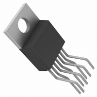
LT1210CT7 Linear Technology, LT1210CT7 Datasheet

LT1210CT7
Specifications of LT1210CT7
Available stocks
Related parts for LT1210CT7
LT1210CT7 Summary of contents
Page 1
... The LT1210 is available in the TO-220 and DD packages for operation with supplies up to ±15V. For ±5V applica- tions the device is also available in a low thermal resis- tance SO-16 package. , LT, LTC and LTM are registered trademarks of Linear Technology Corporation. All other trademarks are the property of their respective owners 100Ω ...
Page 2
... FRONT VIEW 7 OUT – COMP + V 4 SHUTDOWN 3 TAB 2 + – PACKAGE 7-LEAD TO-220 θ = 5°C/W JC ORDER PART NUMBER LT1210CT7 = 0V, unless SD MIN TYP MAX UNITS ±3 ±15 mV ±20 ● mV µV/°C ● 10 ±2 ±5 µA ±20 µA ● ±10 ±60 µA ±100 µA ● ...
Page 3
ELECTRICAL CHARACTERISTICS temperature range, otherwise specifications are at T otherwise noted. SYMBOL PARAMETER CMRR Common Mode Rejection Ratio Inverting Input Current Common Mode Rejection PSRR Power Supply Rejection Ratio Noninverting Input Current Power Supply Rejection Inverting Input Current Power Supply ...
Page 4
LT1210 SMALL-SIGNAL BANDWIDTH = ±5V, Peaking ≤ 1dB R = 0Ω 30mA – 1 150 549 30 590 10 619 1 150 604 30 649 ...
Page 5
W U TYPICAL PERFOR A CE CHARACTERISTICS Bandwidth vs Supply Voltage 100 PEAKING ≤ 1dB PEAKING ≤ 5dB R = 100Ω 470Ω 560Ω ...
Page 6
LT1210 W U TYPICAL PERFOR A CE CHARACTERISTICS Supply Current vs Supply Voltage 0Ω 25° 85° –40° 125°C A ...
Page 7
W U TYPICAL PERFOR A CE CHARACTERISTICS Output Impedance vs Frequency 100 = ±15V 0mA 82. 0Ω 0.1 0.01 100k 1M 10M 100M FREQUENCY (Hz) 1210 G19 ...
Page 8
LT1210 PPLICATI S I FOR ATIO The LT1210 is a current feedback amplifier with high output current drive capability. The device is stable with large capacitive loads and can easily supply the high currents required by ...
Page 9
PPLICATI S I FOR ATIO 15V + V IN LT1210 – SD –15V 5V 74C906 24k 15V ENABLE Figure 2. Shutdown Interface up the turn-off time and ensures that the LT1210 is completely turned off. Because ...
Page 10
LT1210 PPLICATI S I FOR ATIO the bandwidth is reduced. The photos in Figures 5a, 5b and 5c show the large-signal response of the LT1210 for various gain configurations. The slew rate varies from 770V/µs for ...
Page 11
PPLICATI S I FOR ATIO Power Supplies The LT1210 will operate from single or split supplies from ±5V (10V total) to ±15V (30V total not necessary to use equal value split supplies, however the ...
Page 12
LT1210 PPLICATI S I FOR ATIO A T7 Package, 7-Lead TO-220 Thermal Resistance (Junction-to-Case) = 5°C/W Calculating Junction Temperature The junction temperature can be calculated from the equation )(θ ...
Page 13
U TYPICAL APPLICATIONS Distribution Amplifier + V IN LT1210 75Ω SD – PLIFIED SCHE ATIC TO ALL CURRENT SOURCES Q18 Q17 1.25k SHUTDOWN + V 75Ω CABLE IN 75Ω LT1210 – 75Ω 75Ω ...
Page 14
LT1210 PACKAGE DESCRIPTION .060 .256 (1.524) (6.502) .060 .183 (1.524) (4.648) .075 (1.905) .300 (7.620) BOTTOM VIEW OF DD PAK HATCHED AREA IS SOLDER PLATED COPPER HEAT SINK .420 .050 RECOMMENDED SOLDER PAD LAYOUT NOTE: 1. DIMENSIONS IN INCH/(MILLIMETER) 2. ...
Page 15
... BSC (1.27) Information furnished by Linear Technology Corporation is believed to be accurate and reliable. However, no responsibility is assumed for its use. Linear Technology Corporation makes no represen- tation that the interconnection of its circuits as described herein will not infringe on existing patent rights Package 16-Lead Plastic Small Outline (Narrow .150 Inch) (Reference LTC DWG # 05-08-1610) .045 ± ...
Page 16
... Shutdown Function, 1100V/µs Slew Rate Voltage Feedback, Stable with C Voltage Feedback, Stable with C www.linear.com ● Frequency Response –1 –4 10k 100k 1M 10M 100M FREQUENCY (Hz) 1210 TA08 = 10,000pF, 900V/µ 10,000pF L = 10,000pF L LT 0406 REV A • PRINTED IN USA © LINEAR TECHNOLOGY CORPORATION 1996 1210fa ...


