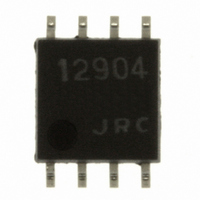
NJM12904M-TE1# NJR, NJM12904M-TE1# Datasheet

NJM12904M-TE1#
Specifications of NJM12904M-TE1#
NJM#12904M-TE1TR
NJM#12904M-TE1TR
NJM12904M-TE1#TR
Related parts for NJM12904M-TE1#
NJM12904M-TE1# Summary of contents
Page 1
... NJM12904D/12904M NJM12904E/12904V/12904R ■ EQUIVALENT CIRCUIT (1/2Shown) - INPUT +INPUT - + + - NJM12904L NJM12904 ■ PACKAGE OUTLINE NJM12904D NJM12904M NJM12904E NJM12904V NJM12904R NJM12904L PIN FUNCTION 1. A OUTPUT 2. A -INPUT 3. A +INPUT 4. GND 5. B +INPUT 6. B -INPUT 7. B OUTPUT + OUTPUT V - ...
Page 2
ABSOLUTE MAXIMUM RATING PARAMETER Supply Voltage Differential Input Voltage Input Voltage Power Dissipation Operating Temperature Range Storage Temperature Range ■ ELECTRICAL CHARACTERISTICS ( V PARAMETER Operating Voltage Input Offset Voltage Input Offset Current Input Bias Current Large Signal Voltage ...
Page 3
TYPICAL CHARACTERISTICS NJM12904 Operating Current v.s Operating Voltage 2 1.8 1.6 1.4 1.2 1 0.8 0.6 0.4 0 Operating Voltage V+/V- (V) NJM12904 Input Bias Current v.s Operating Voltage 100 ...
Page 4
NJM12904 Maximum Output Voltage Swing v.s Load Resistance 4 3.5 3 2.5 2 1.5 1 0.5 0 100 1000 10000 Load Resistance RL (Ω) NJM12904 Output Voltage v.s Output Sink Current 0.01 0.1 1 Output Sink Current Isink (mA) ...
Page 5
NJM12904 Voltage Gain v.s Operating Voltage 160 140 120 100 80 RL=2kΩ Operating Voltage V+ (V) NJM12904 Slew Rate(Fall) Time t (μ 100 ...
Page 6
NJM12904 Operating Current v.s Ambient Temperature 1.4 1.2 V+/V-=6V V+/V-=2.5V 1 0.8 0.6 V+/V-=1.5V 0.4 0.2 0 -50 - Ambient Temperature Ta (℃) NJM12904 Input Bias Current v.s Ambient Temperature 100 V+/V-=1.5V,2.5V, ...
Page 7
NJM12904 Voltage Gain v.s Ambient Temperature 120 100 80 V+/V-=2. -50 - Ambient Temperature Ta (℃) NJM12904 Supply Voltage Rejection Ratio v.s Ambient Temperature 120 100 80 V+/V-=2. -50 - ...
Page 8
MEMO NJM12904 [CAUTION] The specifications on this databook are only given for information , without any guarantee as regards either mistakes or omissions. The application circuits in this databook are described only to show representative usages of the product and ...


