NJM5534D# NJR, NJM5534D# Datasheet
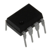
IC OPAMP SINGLE LOW-NOISE 8-DIP

NJM5534D#

Manufacturer Part Number
NJM5534D#
Description
IC OPAMP SINGLE LOW-NOISE 8-DIP
Manufacturer
NJR
Datasheet

Specifications of NJM5534D#

Amplifier Type
General Purpose
Number Of Circuits
1
Slew Rate
13 V/µs
Gain Bandwidth Product
10MHz
Current - Input Bias
500nA
Voltage - Input Offset
500µV
Current - Supply
4mA
Voltage - Supply, Single/dual (±)
±3 V ~ 22 V
Operating Temperature
-20°C ~ 75°C
Mounting Type
Through Hole
Package / Case
8-DIP
Lead Free Status / RoHS Status
Lead free / RoHS Compliant
Output Type
-
Current - Output / Channel
-
-3db Bandwidth
-
Other names
NJM#5534D
NJM#5534D

Available stocks

Company
Part Number
Manufacturer
Quantity
Price
Company:
Part Number:
NJM5534D#NJM5534D
Manufacturer:
JRC
Quantity:
474
Company:
Part Number:
NJM5534D#NJM5534DD
Manufacturer:
NJR
Quantity:
1 842
■ GENERAL DESCRIPTION
This amplifier features popular pin-out, superior noise performance,
and high output drive capability. And also, features guaranteed noise
performance with substantially higher gain-bandwidth product, power
bandwidth, and slew rate which far exceeds that of the NJM741 type
amplifiers.
NJM5534 to be used in very low noise signal processing applications
such as audio pre-amplifiers and servo error amplifiers.
The NJM5534 is internally compensated for a gain of three or higher.
Externally compensation for optimizing specific performance can be
obtained by use of an external compensation capacitor between
COMPENSATION(5PIN) and BALANCE/COMPENSATION(8PIN).
recommended D-Rank type products(NJM5534DD/MD). These
have specified maximum limits for equivalent input noise voltage.
■ FEATURES
■ PIN CONFIGURATION
■ EQUIVALENT CIRCUIT
Ver.2011-02-22
The NJM5534 is a high performance low noise operational amplifier.
The specially designed low noise input transistors allow the
If very low noise characteristic is of prime importance, it is
● Operating Voltage
● Single Circuit
● With BALANCE Terminal
● Low Input Noise Voltage
● Power Bandwidth
● Slew Rate
● Package Outline
● Bipolar Technology
HIGH PERFORMANCE LOW-NOISE OPERATIONAL AMPLIFIER
DIP8, DMP8 Package
±3V~±22V
3.3nV/√Hz typ.@1kHz
200kHz typ.
13V/µs typ.
DIP8, DMP8
1
2
3
4
(Top view)
8
7
6
5
PIN FUNCTION
1.BALANCE
2.–INPUT
3.+INPUT
4.V
5.COMPENSATION
6.OUTPUT
7.V
8.BALANCE/COMPENSATION
-
+
■ PACKAGE OUTLINE
NJM5534D
(DIP8)
NJM5534M
(DMP8)
- 1 -

Related parts for NJM5534D#

NJM5534D# Summary of contents

Page 1

HIGH PERFORMANCE LOW-NOISE OPERATIONAL AMPLIFIER ■ GENERAL DESCRIPTION The NJM5534 is a high performance low noise operational amplifier. This amplifier features popular pin-out, superior noise performance, and high output drive capability. And also, features guaranteed noise performance with substantially higher ...

Page 2

ABSOLUTE MAXIMUM RATINGS (Ta=25˚C) PARAMETER Supply Voltage Differential Input Voltage Common Mode Input Voltage Power Dissipation Operating Temperature Range Storage Temperature Range ■ RECOMMENDED OPERATING VOLTAGE (Ta=25˚C) PARAMETER Supply Voltage ■ ELECTRICAL CHARACTERISTICS (Ta=25˚C,V PARAMETER Input Offset Voltage Input ...

Page 3

TYPICAL CHARACTERISTICS Gain/Phase vs. Frequency Ta=25ºC 50 Gain 40 Phase -10 -20 10k 100k 1M Frequency [Hz] Maximum Output Voltage Swing vs. Frequency + - V /V =±15V, Ta=25º ...

Page 4

TYPICAL CHARACTERISTICS Supply Current vs. Temperature + - V /V =±15V -50 - Ambient Temperature [ºC] Input Bias Current vs. Temperature + - V /V =±15V ...

Page 5

TEST CIRCUIT Noise Voltage (RIAA) measurement circuit 3.3µ ■ ADJUSTMENT METHOD Fig.1-1, Fig.1-2 shows the input offset voltage adjustment circuit, and frequency compensation circuit. Without these features, the adjustment pins are open. Fig.1-1 Input Offset Voltage Adjustment + V ...

Related keywords