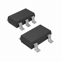
ADA4000-1AUJZ-R2 Analog Devices Inc, ADA4000-1AUJZ-R2 Datasheet

ADA4000-1AUJZ-R2
Specifications of ADA4000-1AUJZ-R2
Related parts for ADA4000-1AUJZ-R2
ADA4000-1AUJZ-R2 Summary of contents
Page 1
... Additional applications for the ADA4000-1/ADA4000-2/ ADA4000-4 include electronic instruments, ATE amplification, buffering, integrator circuits, instrumentation-quality photodiode amplification, and fast precision filters (including PLL filters). The parts also include utility functions, such as reference buffering, level shifting, control I/O interface, power supply control, and monitoring functions ...
Page 2
... ADA4000-1/ADA4000-2/ADA4000-4 TABLE OF CONTENTS Features .............................................................................................. 1 Applications ....................................................................................... 1 General Description ......................................................................... 1 Pin Configurations ........................................................................... 1 Revision History ............................................................................... 2 Specifications ..................................................................................... 3 Electrical Characteristics ............................................................. 3 Absolute Maximum Ratings ............................................................ 5 Thermal Resistance ...................................................................... 5 REVISION HISTORY 3/09—Rev Rev. A Changes to Input Voltage Range Parameter ................................. 4 Changes to Common-Mode Rejection Ration Parameter .......... 4 Updated Outline Dimensions ....................................................... 12 Changes to Ordering Guide .......................................................... 14 5/07—Revision 0: Initial Version Power Sequencing ...
Page 3
... Supply Current/Amplifier DYNAMIC PERFORMANCE Slew Rate Gain Bandwidth Product Phase Margin NOISE PERFORMANCE Voltage Noise Voltage Noise Density Current Noise Density INPUT IMPEDANCE Differential Mode Common Mode ADA4000-1/ADA4000-2/ADA4000-4 Symbol Conditions V OS −40°C ≤ T ≤ +125° −40°C ≤ T ≤ +85°C A − ...
Page 4
... ADA4000-1/ADA4000-2/ADA4000 ± 25°C, unless otherwise specified Table 2. Parameter INPUT CHARACTERISTICS Offset Voltage Input Bias Current Input Offset Current Input Voltage Range Common-Mode Rejection Ratio Open-Loop Gain Offset Voltage Drift OUTPUT CHARACTERISTICS Output Voltage High Output Voltage Low Short-Circuit Current POWER SUPPLY ...
Page 5
... Exposure to absolute maximum rating conditions for extended periods may affect device reliability. ADA4000-1/ADA4000-2/ADA4000-4 THERMAL RESISTANCE θ is specified for the worst-case conditions, that is, a device JA Rating soldered in a circuit board for surface-mount packages ...
Page 6
... ADA4000-1/ADA4000-2/ADA4000-4 TYPICAL PERFORMANCE CHARACTERISTICS ±15V 25° –2.0 –1.5 –1.0 –0.5 0 0.5 OFFSET VOLTAGE (mV) Figure 7. Input Offset Voltage Distribution TCV (µV/°C) OS Figure 8. Offset Voltage Drift Distribution –20 1k 10k 100k 1M FREQUENCY (Hz) Figure 9. Open-Loop Gain and Phase Margin vs. Frequency, V 1.0 1.5 2.0 = ±15 V ...
Page 7
... FREQUENCY (Hz) Figure 13. Common-Mode Rejection Ratio vs. Frequency –5 –10 –15 TIME (1µs/DIV) Figure 14. Large Signal Transient Response, V TIME (2µs/DIV) Figure 15. Small Signal Transient Response, V ADA4000-1/ADA4000-2/ADA4000-4 100 V = ±15V 25° 10M ±15 V Figure 16. Common-Mode Rejection Ratio vs. Frequency ±15V 2kΩ ...
Page 8
... ADA4000-1/ADA4000-2/ADA4000-4 3 25°C A 3.0 2.5 2.0 1.5 1.0 ±5 ±6 ±7 ±8 ±9 ±10 ±11 SUPPLY VOLTAGE (V) Figure 19. Input Bias Current vs. Supply Voltage 10000 1000 100 ±15V ±5V S 0.1 –40 –25 – TEMPERATURE (°C) Figure 20. Input Bias Current vs. Temperature 1.44 1. ± ...
Page 9
... FREQUENCY (Hz) Figure 26. Output Impedance vs. Frequency 100mV p ±5V, ±15V +OVERSHOOT 30 –OVERSHOOT 200 400 600 LOAD CAPACITANCE (pF) Figure 27. Overshoot vs. Load Capacitance ADA4000-1/ADA4000-2/ADA4000-4 0 ±5V, ±15V 25°C A 0.4 0.2 0 –0.2 –0.4 –0.6 10k – ±15V 25° –10 –20 –30 100 10M 100M ...
Page 10
... R change, and the optimum value can be determined empirically. In Figure 31, the oscilloscope image shows the output of the ADA4000-x family in response to a 400 mV pulse. The circuit is configured in the unity gain configuration with 500 pF in parallel with 10 kΩ of load capacitive. ...
Page 11
... DAC t AMP The ADA4000-1/ADA4000-2/ADA4000-4 settle to within 0.1% of their final value in less than 1.2 μs. The settling time has been tested by using the configuration circuit in Figure 34. V1 10V p-p The input signal pulse and the output is the error signal for the settling time shown in Figure 33. ...
Page 12
... ADA4000-1/ADA4000-2/ADA4000-4 OUTLINE DIMENSIONS 0.25 (0.0098) 0.10 (0.0040) COPLANARITY 1.60 BSC * 0.90 MAX 0.70 MIN 0.10 MAX 5.00 (0.1968) 4.80 (0.1890 6.20 (0.2441) 4.00 (0.1574) 1 5.80 (0.2284) 3.80 (0.1497) 4 1.27 (0.0500) BSC 1.75 (0.0688) 1.35 (0.0532) 8° 0° 0.51 (0.0201) 0.10 0.31 (0.0122) ...
Page 13
... MAX 0.80 0.09 0.15 SEATING 0.05 0.30 PLANE COPLANARITY 0.19 0.10 COMPLIANT TO JEDEC STANDARDS MO-153-AB-1 Figure 38. 14-Lead Standard Small Outline Package [TSSOP] (RU-14) Dimensions shown in millimeters Rev Page ADA4000-1/ADA4000-2/ADA4000-4 0.80 8° 0.60 0° 0.40 0.75 8° 0.60 0° 0.45 ...
Page 14
... ORDERING GUIDE Model Temperature Range 1 ADA4000-1ARZ −40°C to +125°C 1 ADA4000-1ARZ-R7 −40°C to +125°C 1 ADA4000-1ARZ-RL −40°C to +125°C ADA4000-1AUJZ-R2 1 −40°C to +125°C 1 ADA4000-1AUJZ-R7 −40°C to +125°C ADA4000-1AUJZ-RL 1 −40°C to +125°C 1 ADA4000-2ARZ −40°C to +125°C ADA4000-2ARZ-R7 1 − ...
Page 15
... NOTES ADA4000-1/ADA4000-2/ADA4000-4 Rev Page ...
Page 16
... ADA4000-1/ADA4000-2/ADA4000-4 NOTES ©2007—2009 Analog Devices, Inc. All rights reserved. Trademarks and registered trademarks are the property of their respective owners. D05791-0-3/09(A) Rev Page ...


