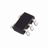
AD8628AUJ-REEL7 Analog Devices Inc, AD8628AUJ-REEL7 Datasheet

AD8628AUJ-REEL7
Specifications of AD8628AUJ-REEL7
Available stocks
Related parts for AD8628AUJ-REEL7
AD8628AUJ-REEL7 Summary of contents
Page 1
FEATURES Lowest auto-zero amplifier noise Low offset voltage: 1 μV Input offset drift: 0.002 μV/°C Rail-to-rail input and output swing 5 V single-supply operation High gain, CMRR, and PSRR: 130 dB Very low input bias current: 100 pA maximum Low ...
Page 2
AD8628/AD8629/AD8630 TABLE OF CONTENTS Features .............................................................................................. 1 Applications....................................................................................... 1 General Description ......................................................................... 1 Pin Configurations ........................................................................... 1 Revision History ............................................................................... 2 Specifications..................................................................................... 3 Electrical Characteristics—V = 5.0 V....................................... 3 S Electrical Characteristics—V = 2.7 V....................................... 4 S Absolute Maximum Ratings............................................................ ...
Page 3
SPECIFICATIONS ELECTRICAL CHARACTERISTICS— 5 2 25°C, unless otherwise noted Table 1. Parameter INPUT CHARACTERISTICS Offset Voltage Input Bias Current AD8628/AD8629 AD8630 Input Offset Current Input Voltage Range Common-Mode Rejection ...
Page 4
AD8628/AD8629/AD8630 ELECTRICAL CHARACTERISTICS— Table 2. Parameter INPUT CHARACTERISTICS Offset Voltage Input Bias Current AD8628/AD8629 AD8630 Input Offset Current Input Voltage Range Common-Mode Rejection ...
Page 5
ABSOLUTE MAXIMUM RATINGS Table 3. Parameter Supply Voltage Input Voltage 1 Differential Input Voltage Output Short-Circuit Duration to GND Storage Temperature Range Operating Temperature Range Junction Temperature Range Lead Temperature (Soldering, 60 sec) ESD AD8628 HBM 8-Lead SOIC FICDM 8-Lead ...
Page 6
AD8628/AD8629/AD8630 TYPICAL PERFORMANCE CHARACTERISTICS 180 V = 2.7V S 160 T = 25°C A 140 120 100 –2.5 –1.5 –0.5 0.5 INPUT OFFSET VOLTAGE (µV) Figure 5. Input Offset Voltage Distribution ...
Page 7
V = 2.7V S 100 10 SOURCE SINK 1 0.1 0.01 0.0001 0.001 0.01 0.1 LOAD CURRENT (mA) Figure 11. Output Voltage to Supply Rail vs. Load Current 1500 2. ...
Page 8
AD8628/AD8629/AD8630 100 –10 –20 –30 1k 10k 100k FREQUENCY (Hz) Figure 17. Closed-Loop Gain vs. Frequency ...
Page 9
V = ±1.35V 50pF ∞ TIME (4µs/DIV) Figure 23. Small Signal Transient Response V = ±2. 50pF ∞ ...
Page 10
AD8628/AD8629/AD8630 V = ±2. 1kHz @ ±3V p 0pF 10kΩ TIME (200µs/DIV) Figure 29. No Phase Reversal 140 V = 2.7V S 120 100 80 ...
Page 11
FREQUENCY (Hz) Figure 35. Maximum Output Swing vs. Frequency 0. 2.7V S 0.45 0.30 0.15 0 –0.15 –0.30 –0.45 –0. ...
Page 12
AD8628/AD8629/AD8630 120 NOISE AT 10kHz = 36.4nV 105 FREQUENCY (kHz) Figure 41. Voltage Noise Density from kHz 120 ...
Page 13
– 1kΩ 100 V – 1kΩ – 10kΩ – 10kΩ – 100kΩ ...
Page 14
AD8628/AD8629/AD8630 FUNCTIONAL DESCRIPTION The AD8628/AD8629/AD8630 are single-supply, ultrahigh precision rail-to-rail input and output operational amplifiers. The typical offset voltage of less than 1 μV allows these amplifiers to be easily configured for high gains without risk of excessive output voltage ...
Page 15
PEAK-TO-PEAK NOISE Because of the ping-pong action between auto-zeroing and chopping, the peak-to-peak noise of the AD8628/AD8629/ AD8630 is much lower than the competition. Figure 50 and Figure 51 show this comparison. e p-p = 0.5µ 0.1Hz ...
Page 16
AD8628/AD8629/AD8630 INPUT OVERVOLTAGE PROTECTION Although the AD8628/AD8629/AD8630 are rail-to-rail input amplifiers, care should be taken to ensure that the potential difference between the inputs does not exceed the supply voltage. Under normal negative feedback operating conditions, the amplifier corrects its ...
Page 17
CH1 = 50mV/DIV CH2 = 1V/DIV OUT 0V TIME (500µs/DIV) Figure 59. Negative Input Overload Recovery for the AD8628 0V CH1 = 50mV/DIV CH2 = 1V/DIV OUT 0V TIME (500µs/DIV) Figure ...
Page 18
AD8628/AD8629/AD8630 PRECISION CURRENT SHUNT SENSOR A precision current shunt sensor benefits from the unique attributes of auto-zero amplifiers when used in a differencing configuration, as shown in Figure 63. Current shunt sensors are used in precision current sources for feedback ...
Page 19
OUTLINE DIMENSIONS 2.90 BSC 5 4 2.80 BSC 1.60 BSC 0.95 BSC 1.90 * 0.90 MAX BSC 0.70 MIN * 1.00 MAX 0.20 0.08 0.10 MAX 0.50 SEATING PLANE 0.30 * COMPLIANT TO JEDEC STANDARDS MO-193-AB WITH ...
Page 20
AD8628/AD8629/AD8630 8.75 (0.3445) 8.55 (0.3366 6.20 (0.2441) 4.00 (0.1575) 1 5.80 (0.2283) 3.80 (0.1496) 7 1.27 (0.0500) BSC 1.75 (0.0689) 0.25 (0.0098) 1.35 (0.0531) 0.10 (0.0039) COPLANARITY SEATING 0.51 (0.0201) 0.10 PLANE 0.25 (0.0098) 0.31 (0.0122) 0.17 (0.0067) ...
Page 21
... ORDERING GUIDE 1, 2 Model Temperature Range AD8628AUJ-REEL −40°C to +125°C AD8628AUJ-REEL7 −40°C to +125°C AD8628AUJZ-R2 −40°C to +125°C AD8628AUJZ-REEL −40°C to +125°C AD8628AUJZ-REEL7 −40°C to +125°C AD8628ARZ −40°C to +125°C AD8628ARZ-REEL −40°C to +125°C AD8628ARZ-REEL7 − ...
Page 22
AD8628/AD8629/AD8630 NOTES Rev Page ...
Page 23
NOTES AD8628/AD8629/AD8630 Rev Page ...
Page 24
AD8628/AD8629/AD8630 NOTES ©2002–2011 Analog Devices, Inc. All rights reserved. Trademarks and registered trademarks are the property of their respective owners. D02735-0-4/11(I) Rev Page ...


