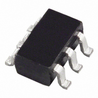
AD8027ARTZ-R2 Analog Devices Inc, AD8027ARTZ-R2 Datasheet

AD8027ARTZ-R2
Specifications of AD8027ARTZ-R2
Available stocks
Related parts for AD8027ARTZ-R2
AD8027ARTZ-R2 Summary of contents
Page 1
FEATURES High speed 190 MHz, –3 dB bandwidth (G = +1) 100 V/μs slew rate Low distortion 120 dBc @ 1 MHz SFDR 80 dBc @ 5 MHz SFDR Selectable input crossover threshold Low noise 4.3 nV/√Hz 1.6 pA/√Hz Low ...
Page 2
AD8027/AD8028 TABLE OF CONTENTS Specifications..................................................................................... 3 Absolute Maximum Ratings............................................................ 6 Maximum Power Dissipation ..................................................... 6 ESD Caution.................................................................................. 6 Typical Performance Characteristics ............................................. 8 Theory of Operation ...................................................................... 17 Input Stage................................................................................... 17 Crossover Selection .................................................................... 17 Output Stage................................................................................ 18 DC Errors ...
Page 3
SPECIFICATIONS V = ± 25° kΩ to midsupply unless otherwise noted Table 1. Parameter DYNAMIC PERFORMANCE –3 dB Bandwidth Bandwidth for 0.1 dB Flatness Slew Rate Settling ...
Page 4
AD8027/AD8028 25° kΩ to midsupply, unless otherwise noted Table 2. Parameter DYNAMIC PERFORMANCE −3 dB Bandwidth Bandwidth for 0.1 dB Flatness Slew Rate Settling Time to 0.1% ...
Page 5
25° kΩ to midsupply, unless otherwise noted Table 3. Parameter DYNAMIC PERFORMANCE –3 dB Bandwidth Bandwidth for 0.1 dB Flatness Slew Rate Settling Time to 0.1% NOISE/DISTORTION ...
Page 6
AD8027/AD8028 ABSOLUTE MAXIMUM RATINGS Table 4. Parameter Rating Supply Voltage 12.6 V Power Dissipation See Figure 3 Common-Mode Input Voltage ±V Differential Input Voltage ±1.8 V Storage Temperature –65°C to +125°C Operating Temperature Range –40°C to +125°C 300°C Lead Temperature ...
Page 7
Figure 3 shows the maximum safe power dissipation in the package vs. the ambient temperature for the SOIC-8 (125°C/W), SOT-23-6 (170°C/W), and MSOP-10 (130°C/W) packages on a JEDEC standard 4-layer board. Output Short Circuit Shorting the output to ground or ...
Page 8
AD8027/AD8028 TYPICAL PERFORMANCE CHARACTERISTICS Default conditions 25° 200mV p-p OUT 1 0 –1 –2 –3 –4 – +10 –6 –7 –8 –9 –10 0.1 1 ...
Page 9
200mV p-p OUT –1 –2 – 0pF L –4 –5 –6 –7 –8 0 FREQUENCY (MHz) Figure 10. AD8027 Small Signal Frequency Response for Various C ...
Page 10
AD8027/AD8028 0.3V ICM S– 200mV p-p OUT SELECT = TRI – 0.2V ICM S+ SELECT = HIGH 1 0 – 0.2V ...
Page 11
24.9Ω) F FREQUENCY = 100kHz R = 1kΩ L –40 – –80 –100 –120 SECOND HARMONIC: SOLID LINE THIRD HARMONIC: DASHED LINE –140 ...
Page 12
AD8027/AD8028 0. ± 2.5V S 0.15 0.10 0.05 0 –0.05 –0.10 –0.15 50mV/DIV –0.20 Figure 28. Small Signal Transient Response p-p OUT 2 ±2. ...
Page 13
(200mV/DIV – 2V (2mV/DIV) OUT IN Figure 34. Long-Term Settling Time V (200mV/DIV (400mV/DIV) OUT V – 2V (0.1%/DIV) OUT IN Figure 35. 0.1% Short-Term Settling Time 4.5 4.0 SELECT = HIGH ...
Page 14
AD8027/AD8028 290 270 SELECT = HIGH 250 230 210 SELECT = TRI 190 170 150 –5 –4 –3 –2 – INPUT COMMON-MODE VOLTAGE (V) Figure 40. Input Offset Voltage vs. Input Common-Mode Voltage, V 290 V = +5V ...
Page 15
LOAD RESISTANCE TIED TO MIDSUPPLY 150 100 V – ± – –100 –150 –200 100 1000 LOAD RESISTANCE (Ω) Figure 46. Output ...
Page 16
AD8027/AD8028 1.5 SELECT PIN (–2.0V TO –0.5V) 1.0 OUTPUT 0 100Ω 1kΩ L –0 10kΩ L –1.0 –1 100 150 TIME (ns) Figure 52. Enable Turn-On Timing 1.5 SELECT PIN ...
Page 17
THEORY OF OPERATION The AD8027/AD8028 are rail-to-rail input/output amplifiers designed in the Analog Devices XFCB process. The XFCB process enables the AD8027/AD8028 to run on 2 supplies with 190 MHz of bandwidth and over 100 V/μs ...
Page 18
AD8027/AD8028 In the event that the crossover region cannot be avoided, specific attention has been given to the input stage to ensure constant transconductance and minimal offset in all regions of operation. The regions are PNP input pair running, NPN ...
Page 19
WIDEBAND OPERATION Voltage feedback amplifiers can use a wide range of resistor values to set their gain. Proper design of the application’s feedback network requires consideration of the following issues: • Poles formed by the amplifier’s input capacitances with the ...
Page 20
AD8027/AD8028 PCB Layout As with all high speed op amps, achieving optimum perform- ance from the AD8027/AD8028 requires careful attention to PCB layout. Particular care must be exercised to minimize lead lengths of the bypass capacitors. Excess lead inductance can ...
Page 21
APPLICATIONS USING THE SELECT PIN The AD8027/AD8028’s unique SELECT pin has two functions: • The power-down function places the AD8027/AD8028 into low power consumption mode. In power-down mode, the amplifiers draw 450 μA (typical) of supply current. • The second ...
Page 22
AD8027/AD8028 BAND-PASS FILTER In communication systems, active filters are used extensively in signal processing. The AD8027/AD8028 are excellent choices for active filter applications. In realizing this filter impor- tant that the amplifier have a large signal bandwidth of ...
Page 23
OUTLINE DIMENSIONS 0.15 MAX 5.00 (0.1968) 4.80 (0.1890 6.20 (0.2440) 4.00 (0.1574) 5.80 (0.2284) 3.80 (0.1497 1.27 (0.0500) BSC 1.75 (0.0688) 1.35 (0.0532) 0.25 (0.0098) 0.10 (0.0040) 0.51 (0.0201) COPLANARITY 0.25 (0.0098) 0.31 (0.0122) SEATING 0.10 ...
Page 24
... ORDERING GUIDE Minimum Model Ordering Quantity AD8027AR 1 AD8027AR-REEL 2,500 AD8027AR-REEL7 1,000 1 AD8027ARZ 1 1 AD8027ARZ-REEL 2,500 AD8027ARZ-REEL7 1 1,000 AD8027ART-R2 250 AD8027ART-REEL 10,000 AD8027ART-REEL7 3,000 1 AD8027ARTZ-R2 250 1 AD8027ARTZ-REEL 10,000 1 AD8027ARTZ-REEL7 3,000 AD8028AR 1 AD8028AR-REEL 2,500 AD8028AR-REEL7 1,000 1 AD8028ARZ 1 AD8028ARZ-REEL 1 2,500 1 AD8028ARZ-REEL7 1,000 AD8028ARM 1 AD8028ARM-REEL ...


