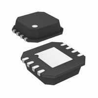
AD8045ACPZ-R2 Analog Devices Inc, AD8045ACPZ-R2 Datasheet - Page 16

AD8045ACPZ-R2
Manufacturer Part Number
AD8045ACPZ-R2
Description
IC OPAMP VF ULDIST LN 8LFCSP
Manufacturer
Analog Devices Inc
Datasheet
1.AD8045ACPZ-REEL7.pdf
(24 pages)
Specifications of AD8045ACPZ-R2
Slew Rate
1350 V/µs
Amplifier Type
Voltage Feedback
Number Of Circuits
1
-3db Bandwidth
1GHz
Current - Input Bias
2µA
Voltage - Input Offset
200µV
Current - Supply
16mA
Current - Output / Channel
70mA
Voltage - Supply, Single/dual (±)
3.3 V ~ 12 V, ±1.65 V ~ 6 V
Operating Temperature
-40°C ~ 125°C
Mounting Type
Surface Mount
Package / Case
8-LFCSP
Op Amp Type
Low Distortion
No. Of Amplifiers
1
Bandwidth
1MHz
Supply Voltage Range
3.3V To 12V
Amplifier Case Style
LFCSP
No. Of Pins
8
Operating Temperature Range
-40°C To
Lead Free Status / RoHS Status
Lead free / RoHS Compliant
Output Type
-
Gain Bandwidth Product
-
Lead Free Status / RoHS Status
Lead free / RoHS Compliant, Lead free / RoHS Compliant
AD8045
CIRCUIT CONFIGURATIONS
WIDEBAND OPERATION
Figure 61 and Figure 62 show the recommended circuit
configurations for noninverting and inverting amplifiers. In
unity gain (G = +1) applications, R
frequency peaking. It is not needed for any other configurations.
For more information on layout, see the Printed Circuit Board
Layout section.
The resistor at the output of the amplifier, labeled R
only when driving large capacitive loads. Using R
stability and minimizes ringing at the output. For more infor-
mation, see the Driving Capacitive Loads section.
V
IN
Figure 61. Noninverting Configuration
R
R
G
S
AD8045
+V
–V
S
S
R
F
0.1µF
0.1µF
10µF
+
10µF
+
S
helps to reduce high
R
SNUB
V
OUT
SNUB
SNUB
improves
, is used
Rev. A | Page 16 of 24
V
IN
R = R
G
R
||R
G
Figure 62. Inverting Configuration
F
AD8045
+V
–V
S
S
R
F
0.1µF
0.1µF
10µF
10µF
+
+
R
SNUB
V
OUT


