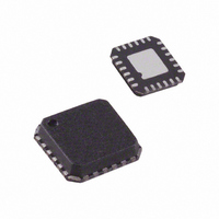
AD8368ACPZ-REEL7 Analog Devices Inc, AD8368ACPZ-REEL7 Datasheet

AD8368ACPZ-REEL7
Specifications of AD8368ACPZ-REEL7
AD8368ACPZ-REEL7TR
Related parts for AD8368ACPZ-REEL7
AD8368ACPZ-REEL7 Summary of contents
Page 1
FEATURES Analog variable gain range: − +22 dB Linear-in-dB scaling: 37.5 dB bandwidth: 800 MHz @ V = 0.5 V GAIN Integrated rms detector P1dB: 16 dBm @ 140 MHz Output IP3: 33 dBm @ 140 ...
Page 2
AD8368 TABLE OF CONTENTS Features ............................................................................................ 1 Applications ..................................................................................... 1 Functional Block Diagram ............................................................ 1 General Description ....................................................................... 1 Revision History ............................................................................. 2 Specifications ................................................................................... 3 Absolute Maximum Ratings .......................................................... 5 ESD Caution ................................................................................ 5 Pin Configuration and Function Descriptions ...
Page 3
SPECIFICATIONS 25°C, system impedance Table 1. Parameter OVERALL FUNCTION Frequency Range Maximum Input 1 Maximum Output AC Input Impedance AC Output Impedance GAIN CONTROL INTERFACE (GAIN) Gain Span Gain Scaling Gain ...
Page 4
AD8368 25°C, system impedance Table 2. Parameter SQUARE LAW DETECTOR (DETI, DETO) Output Setpoint DETI DC Bias Level to ICOM DETI Impedance 1 DETO Output Range AGC Step Response MODE CONTROL ...
Page 5
ABSOLUTE MAXIMUM RATINGS Table 3. Parameter Supply Voltage (VPSO, VPSI) ENBL and MODE Select Voltage RF Input Level Internal Power Dissipation θ JA Maximum Junction Temperature Operating Temperature Range Storage Temperature Range Lead Temperature (Soldering, 60 sec) Stresses above those ...
Page 6
AD8368 PIN CONFIGURATION AND FUNCTION DESCRIPTIONS Table 4. Pin Function Descriptions Pin No. Mnemonic Description 1 GAIN Gain Control. 2 DETO Detector Output. Provides an output error current for the AGC function. 3 HPFL High-Pass Filter Connection. A capacitor to ...
Page 7
TYPICAL PERFORMANCE CHARACTERISTICS 25°C, system impedance 0.75V 10 5 0.5V 0 –5 0.25V –10 0V –15 –20 10 100 FREQUENCY (MHz) Figure 3. S21 vs. Frequency by V ...
Page 8
AD8368 110 150 190 230 RF INPUT (MHz) Figure 9. Output Third-Order Intercept vs. RF Input Frequency at Maximum Gain (V MODE 40 70MHz 240MHz 380MHz 20 ...
Page 9
FREQUENCY (MHz) Figure 15. Noise Figure vs. Frequency at Maximum Gain ( 70MHz 10 140MHz 240MHz 5 380MHz 0 ...
Page 10
AD8368 1.0 0.9 0.8 0.7 0.6 0.5 +85°C 0.4 0.3 +25°C 0.2 0.1 –40°C +85°C 0 –40 –35 –30 –25 –20 –15 RF INPUT (dBm) Figure 21. RSSI (V ) and Conformance Error vs. Input Power ( MHz) ...
Page 11
V ENBL V OUTP CH2 500mV Ω CH3 5V Ω M2.0µs 250MS/s A CH3 4.0ns/PT Figure 27. ENBL Response Time 36.8 37.0 37.2 37.4 37.6 37.8 SLOPE (dB/V) Figure 28. Gain Scaling Distribution (140 ...
Page 12
AD8368 CIRCUIT DESCRIPTION The AD8368 is a single-ended VGA with a bandwidth of 800 MHz and a gain control span ranging from − +22 dB. It incorporates an uncommitted square law detector that can be ...
Page 13
GAIN CONTROL INTERFACE The AD8368 has a linear-in-dB gain control interface that can be operated in either a gain-up mode or gain-down mode. In the gain-up mode with the MODE pin pulled high, the gain increases with increasing gain voltages. ...
Page 14
AD8368 APPLICATIONS INFORMATION VGA OPERATION The AD8368 is a general-purpose VGA suitable for use in a wide variety of applications where accurate, continuous, linear-in-dB gain control over a broad range of frequencies is important. Its stability over temperature and supply ...
Page 15
The output setpoint can be increased using an external resistive divider network between OUTP and DETI, referenced to DECL as depicted in Figure 34. In this configuration, the rms output voltage is forced R1/R2 rms ...
Page 16
AD8368 The choice compromise of averaging time constant, DETO response time, and carrier leakage DETO small to speed up the response time, the AGC loop could start tracking and leveling any amplitude envelope and ...
Page 17
EVALUATION BOARD The standard evaluation board schematic and layout artwork is presented in Figure 41 through Figure 44. The evaluation board is fabricated on a multilayer FR-4 board, with 50 Ω-controlled impedance transmission lines for the RF input and output ...
Page 18
AD8368 Component Function JP4 Jumper for AGC Mode of Operation. Provides feedback from the detector output to the gain pin. SW1 Mode Switch. Low mode puts the part in gain-down mode. High mode puts the part in gain-up mode. AGC ...
Page 19
... OUTLINE DIMENSIONS PIN 1 INDICATOR 1.00 12° MAX 0.85 0.80 SEATING PLANE ORDERING GUIDE Model Temperature Range 1 AD8368ACPZ-REEL7 −40°C to +85° AD8368ACPZ-WP −40°C to +85°C 1 AD8368-EVALZ RoHS Compliant Part waffle pack. 0.60 MAX 4.00 BSC SQ 0.60 MAX 19 18 0.50 BSC TOP 3 ...
Page 20
AD8368 NOTES ©2006–2008 Analog Devices, Inc. All rights reserved. Trademarks and registered trademarks are the property of their respective owners. D05907-0-9/08(B) Rev Page ...


