AD841JNZ Analog Devices Inc, AD841JNZ Datasheet - Page 6
AD841JNZ
Manufacturer Part Number
AD841JNZ
Description
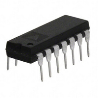
IC OPAMP GP 40MHZ 50MA 14DIP
Manufacturer
Analog Devices Inc
Datasheet
1.AD841JNZ.pdf
(8 pages)
Specifications of AD841JNZ
Slew Rate
300 V/µs
Amplifier Type
General Purpose
Number Of Circuits
1
Gain Bandwidth Product
40MHz
Current - Input Bias
3.5µA
Voltage - Input Offset
800µV
Current - Supply
11mA
Current - Output / Channel
50mA
Voltage - Supply, Single/dual (±)
±5 V ~ 18 V
Operating Temperature
0°C ~ 75°C
Mounting Type
Through Hole
Package / Case
14-DIP (0.300", 7.62mm)
Op Amp Type
Unity Gain Stable
No. Of Amplifiers
1
Bandwidth
40MHz
Supply Voltage Range
± 5V To ± 18V
Amplifier Case Style
DIP
No. Of Pins
14
Lead Free Status / RoHS Status
Lead free / RoHS Compliant
Output Type
-
-3db Bandwidth
-
Lead Free Status / RoHS Status
Lead free / RoHS Compliant, Lead free / RoHS Compliant
Available stocks
Company
Part Number
Manufacturer
Quantity
Price


AD841
OFFSET NULLING
The input offset voltage of the AD841 is very low for a high
speed op amp, but if additional nulling is required, the circuit
shown in Figure 21 can be used.
Figure 19a. Inverting Amplifier
Configuration (DIP Pinout)
Figure 20a. Unity-Gain Buffer Amplifier
Configuration (DIP Pinout)
Figure 21. Offset Nulling (DIP Pinout)
Figure 19b. Inverter Large Signal
Pulse Response
Figure 20b. Buffer Large Signal
Pulse Response
–6–
INPUT CONSIDERATIONS
An input resistor (R
where the input to the AD841 will be subjected to transient or
continuous overload voltages exceeding the 6 V maximum dif-
ferential limit. This resistor provides protection for the input
transistors by limiting the maximum current that can be forced
into the input.
For high performance circuits it is recommended that a resistor
(R
by matching the impedance at each input. The output voltage
error caused by the offset current is more than an order of mag-
nitude less than the error present if the bias current error is not
removed.
AD841 SETTLING TIME
Figures 22 and 24 show the settling performance of the AD841
in the test circuit shown in Figure 23.
Settling time is defined as:
This definition encompasses the major components which com-
prise settling time. They include (1) propagation delay through
the amplifier; (2) slewing time to approach the final output
value; (3) the time of recovery from the overload associated with
slewing and (4) linear settling to within the specified error band.
The interval of time from the application of an ideal step
function input until the closed-loop amplifier output has
entered and remains within a specified error band.
B
in Figures 19 and 20) be used to reduce bias current errors
IN
in Figure 20) is recommended in circuits
Figure 19c. Inverter Small Signal
Pulse Response
Figure 20c. Buffer Small Signal
Pulse Response
REV. B
Related parts for AD841JNZ
Image
Part Number
Description
Manufacturer
Datasheet
Request
R

Part Number:
Description:
±1.7g Dual-Axis IMEMS Accelerometer Evaluation Board
Manufacturer:
Analog Devices Inc
Datasheet:

Part Number:
Description:
Inertial Sensor Evaluation System
Manufacturer:
Analog Devices Inc
Datasheet:
Part Number:
Description:
Manufacturer:
Analog Devices Inc
Datasheet:
Part Number:
Description:
Manufacturer:
Analog Devices Inc
Datasheet:
Part Number:
Description:
Manufacturer:
Analog Devices Inc
Datasheet:
Part Number:
Description:
Manufacturer:
Analog Devices Inc
Datasheet:
Part Number:
Description:
Manufacturer:
Analog Devices Inc
Datasheet:
Part Number:
Description:
Manufacturer:
Analog Devices Inc
Datasheet:
Part Number:
Description:
Manufacturer:
Analog Devices Inc
Datasheet:
Part Number:
Description:
Manufacturer:
Analog Devices Inc
Datasheet:
Part Number:
Description:
Manufacturer:
Analog Devices Inc
Datasheet:
Part Number:
Description:
Manufacturer:
Analog Devices Inc
Datasheet:
Part Number:
Description:
Manufacturer:
Analog Devices Inc
Datasheet: