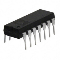
AD841JNZ Analog Devices Inc, AD841JNZ Datasheet - Page 7

AD841JNZ
Manufacturer Part Number
AD841JNZ
Description
IC OPAMP GP 40MHZ 50MA 14DIP
Manufacturer
Analog Devices Inc
Datasheet
1.AD841JNZ.pdf
(8 pages)
Specifications of AD841JNZ
Slew Rate
300 V/µs
Amplifier Type
General Purpose
Number Of Circuits
1
Gain Bandwidth Product
40MHz
Current - Input Bias
3.5µA
Voltage - Input Offset
800µV
Current - Supply
11mA
Current - Output / Channel
50mA
Voltage - Supply, Single/dual (±)
±5 V ~ 18 V
Operating Temperature
0°C ~ 75°C
Mounting Type
Through Hole
Package / Case
14-DIP (0.300", 7.62mm)
Op Amp Type
Unity Gain Stable
No. Of Amplifiers
1
Bandwidth
40MHz
Supply Voltage Range
± 5V To ± 18V
Amplifier Case Style
DIP
No. Of Pins
14
Lead Free Status / RoHS Status
Lead free / RoHS Compliant
Output Type
-
-3db Bandwidth
-
Lead Free Status / RoHS Status
Lead free / RoHS Compliant, Lead free / RoHS Compliant
Available stocks
Company
Part Number
Manufacturer
Quantity
Price
REV. B
Expressed in these terms, the measurement of settling time is obvi-
ously a challenge and needs to be done accurately to assure the
user that the amplifier is worth consideration for the application.
Measurement of the AD841’s 0.01% settling in 110 ns was ac-
complished by amplifying the error signal from a false summing
junction with a very high speed proprietary hybrid error ampli-
fier specially designed to enable testing of small settling errors.
The device under test was driving a 500
the error amp is clamped in order to avoid possible problems as-
sociated with the overdrive recovery of the oscilloscope input
amplifier. The error amp gains the error from the false summing
junction by 10, and it contains a gain vernier to fine trim the
gain.
Figure 24 shows the “long term” stability of the settling charac-
teristics of the AD841 output after a 10 V step. There is no evi-
dence of settling tails after the initial transient recovery time.
The use of a junction isolated process, together with careful lay-
out, avoids these problems by minimizing the effects of transis-
tor isolation capacitance discharge and thermally induced shifts
in circuit operating points. These problems do not occur even
under high output current conditions.
Figure 22. AD841 0.01% Settling Time
Figure 23. Settling Time Test Circuit
load. The input to
–7–
Figure 24. AD841 Settling Demonstrating No Settling
Tails
GROUNDING AND BYPASSING
In designing practical circuits with the AD841, the user must
remember that whenever high frequencies are involved, some
special precautions are in order. Circuits must be built with
short interconnect leads. Large ground planes should be used
whenever possible to provide a low resistance, low inductance
circuit path, as well as minimizing the effects of high frequency
coupling. Sockets should be avoided because the increased
interlead capacitance can degrade bandwidth.
Feedback resistors should be of low enough value to assure that
the time constant formed with the circuit capacitances will not
limit the amplifier performance. Resistor values of less than
5 k are recommended. If a larger resistor must be used, a
small (<10 pF) feedback capacitor in parallel with the feedback
resistor, R
tances and optimize the dynamic performance of the amplifier
in the particular application.
Power supply leads should be bypassed to ground as close as
possible to the amplifier pins. A 2.2 F capacitor in parallel
with a 0.1 F ceramic disk capacitor is recommended.
CAPACITIVE LOAD DRIVING ABILITY
Like all wideband amplifiers, the AD841 is sensitive to capaci-
tive loading. The AD841 is designed to drive capacitive loads of
up to 20 pF without degradation of its rated performance. Ca-
pacitive loads of greater than 20 pF will decrease the dynamic
performance of the part although instability should not occur
unless the load exceeds 100 pF (for a unity-gain follower). A
resistor in series with the output can be used to decouple larger
capacitive loads.
Figure 25 shows a typical configuration for driving a large ca-
pacitive load. The 51
high frequency feedback from the load and stabilizes the circuit.
Low frequency feedback is returned to the amplifier summing
junction via the low pass filter formed by the 51
the load capacitance, C
F
, may be used to compensate for these stray capaci-
L
output resistor effectively isolates the
.
Applying the AD841
resistor and


