AD606JR-REEL7 Analog Devices Inc, AD606JR-REEL7 Datasheet
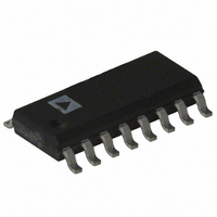
IC AMP LOG LP 1.2MA 16SOIC

AD606JR-REEL7

Manufacturer Part Number
AD606JR-REEL7
Description
IC AMP LOG LP 1.2MA 16SOIC
Manufacturer
Analog Devices Inc
Datasheet

Specifications of AD606JR-REEL7

Rohs Status
RoHS non-compliant
Amplifier Type
Logarithmic
Number Of Circuits
1
Output Type
Differential
Current - Input Bias
4µA
Current - Supply
13mA
Current - Output / Channel
1.2mA
Voltage - Supply, Single/dual (±)
4.5 V ~ 5.5 V
Operating Temperature
0°C ~ 70°C
Mounting Type
Surface Mount
Package / Case
16-SOIC (3.9mm Width)
-3db Bandwidth
-
Slew Rate
-
Gain Bandwidth Product
-
Voltage - Input Offset
-
a
PRODUCT DESCRIPTION
The AD606 is a complete, monolithic logarithmic amplifier
using a 9-stage “successive-detection” technique. It provides
both logarithmic and limited outputs. The logarithmic output is
from a three-pole post-demodulation low-pass filter and provides
REV. B
Information furnished by Analog Devices is believed to be accurate and
reliable. However, no responsibility is assumed by Analog Devices for its
use, nor for any infringements of patents or other rights of third parties
which may result from its use. No license is granted by implication or
otherwise under any patent or patent rights of Analog Devices.
FEATURES
Logarithmic Amplifier Performance
Limiter Performance
Low Power
APPLICATIONS
Ultrasound and Sonar Processing
Phase-Stable Limiting Amplifier to 100 MHz
Received Signal Strength Indicator (RSSI)
Wide Range Signal and Power Measurement
–75 dBm to +5 dBm Dynamic Range
Usable to >50 MHz
37.5 mV/dB Voltage Output
On-Chip Low-Pass Output Filter
Adjustable Output Amplitude
+5 V Single Supply Operation
65 mW Typical Power Consumption
CMOS-Compatible Power-Down to 325 W typ
<5
1.5 nV/ Hz Input Noise
1 dB Output Flatness over 80 dB Range
3 Phase Stability at 10.7 MHz over 80 dB Range
s Enable/Disable Time
INLO
INHI
16
1
30k
1.5k
1.5k
AD606
250
COMM
COMM
15
2
30k
DETECTORS
HIGH-END
AND POWER-UP
REFERENCE
PRUP
FUNCTIONAL BLOCK DIAGRAM
ISUM
14
Logarithmic Amplifier with Limiter Output
3
12 A/dB
2 A/dB
ONE-POLE
FILTER
VPOS
ILOG
13
4
X1
9.375k
9.375k
a loadable output voltage of +0.1 V dc to +4 V dc. The logarith-
mic scaling is such that the output is +0.5 V for a sinusoidal
input of –75 dBm and +3.5 V at an input of +5 dBm; over this
range the logarithmic linearity is typically within 0.4 dB. All
scaling parameters are proportional to the supply voltage.
The AD606 can operate above and below these limits, with
reduced linearity, to provide as much as 90 dB of conversion
range. A second low-pass filter automatically nulls the input
offset of the first stage down to the submicrovolt level. Adding
external capacitors to both filters allows operation at input fre-
quencies as low as a few hertz.
The AD606’s limiter output provides a hard-limited signal
output as a differential current of 1.2 mA from open-collector
outputs. In a typical application, both of these outputs are
loaded by 200
90 dB from the input. Transition times are 1.5 ns, and the
phase is stable to within 3 at 10.7 MHz for signals from
–75 dBm to +5 dBm.
The logarithmic amplifier operates from a single +5 V supply
and typically consumes 65 mW. It is enabled by a CMOS logic
level voltage input, with a response time of <5 s. When dis-
abled, the standby power is reduced to <1 mW within 5 s.
The AD606J is specified for the commercial temperature range
of 0 C to +70 C and is available in 16-lead plastic DIPs or
SOICs. Consult the factory for other packages and temperature
ranges.
One Technology Way, P.O. Box 9106, Norwood, MA 02062-9106, U.S.A.
Tel: 781/329-4700
Fax: 781/326-8703
BFIN
FIL1
30pF
MAIN SIGNAL PATH
12
5
11.15dB/STAGE
2pF
50 MHz, 80 dB Demodulating
LOW-PASS FILTER
30pF
2pF
OFFSET-NULL
X2
VLOG
SALLEN-KEY
FIL2
TWO-POLE
11
6
FILTER
resistors to provide a voltage gain of more than
360k
360k
World Wide Web Site: http://www.analog.com
OPCM
LADJ
10
7
LIMITER
FINAL
LMLO
LMHI
9
8
© Analog Devices, Inc., 1999
AD606

Related parts for AD606JR-REEL7

AD606JR-REEL7 Summary of contents

Page 1

FEATURES Logarithmic Amplifier Performance –75 dBm to +5 dBm Dynamic Range 1.5 nV/ Hz Input Noise Usable to >50 MHz 37.5 mV/dB Voltage Output On-Chip Low-Pass Output Filter Limiter Performance 1 dB Output Flatness over 80 dB Range 3 ...

Page 2

AD606–SPECIFICATIONS Model Parameter Conditions SIGNAL INPUT Log Amp f AC Coupled; Sinusoidal Input MAX Limiter f AC Coupled; Sinusoidal Input MAX Dynamic Range Input Resistance Differential Input Input Capacitance Differential Input SIGNAL OUTPUT Limiter Flatness –75 dBm to +5 dBm ...

Page 3

... Temperature Package Model Range Description AD606JN +70 C 16-Lead Plastic DIP AD606JR +70 C 16-Lead Narrow-Body R-16A SOIC AD606JR-REEL +70 C 13" Tape and Reel AD606JR-REEL7 +70 C 7" Tape and Reel AD606-EB Evaluation Board AD606JCHIPS +70 C Die PIN DESCRIPTION Plastic DIP (N) and Small Outline (R) Packages ...

Page 4

AD606 INPUT LEVEL CONVENTIONS RF logarithmic amplifiers usually have their input specified in “dBm,” meaning “decibels with respect to 1 mW.” Unfortu- nately, this is not precise for several reasons. 1. Log amps respond not to power but to voltage. ...

Page 5

V The slope is essentially independent of temperature. The intercept P is essentially independent of either the supply X voltage or temperature. However, the AD606 is not factory calibrated, and both ...

Page 6

AD606 Offset-Control Loop The offset-control loop nulls the input offset voltage, and sets up the bias voltages at the input pins INHI and INLO. A full understanding of this offset-control loop is useful, particularly when using larger input coupling capacitors ...

Page 7

For operation above 10 MHz not necessary to add the external capacitors CF1, CF2, and C , although an improve- Z ment in low frequency noise can be achieved by so doing (see APPLICATIONS). Note that the offset ...

Page 8

AD606 Adjustment Procedure The slope and intercept adjustments interact; this can be mini- mized by reducing the resistance of R1 and R2, chosen here to minimize power drain. Calibration can be achieved in several ways: The simplest is to apply ...

Page 9

ATTENUATOR AC INPUT R4 453 R5 51.1 DIECAST BOX Figure 8. Circuit for Low Frequency Measurements Low Frequency Applications With reasonably sized input coupling capacitors and an optional input low-pass filter, the AD606 can operate to frequencies as low ...

Page 10

AM AD606–Typical Performance Characteristics 0.5 –0.5 70MHz –1.5 45MHz –2.5 10.7MHz –3.5 –4.5 –5.5 –6.5 –80 –70 –60 –50 –40 –30 –20 – INPUT LEVEL – dBm Figure 10. Normalized Limiter Amplitude Response vs. Input Level ...

Page 11

Figure 19. V Output for a Pulsed LOG 10.7 MHz Input; Top Trace: –35 dBm to +5 dBm; Middle Trace: –15 dBm to –55 dBm; Bottom Trace: –35 dBm to – 75 dBm –10dB TO +30dB (10.7MHz SWEPT GAIN TESTS ...

Page 12

AD606 0.125 (3.18) 0.1574 (4.00) 0.1497 (3.80) OUTLINE DIMENSIONS Dimensions shown in inches and (mm). 16-Lead Plastic DIP (N-16) 0.87 (22.1) MAX 16 9 0.31 (7.87) 0.25 (6.35 0.300 (7.62) 0.35 PIN 1 (0.89) 0.18 0.011 (4.57) (0.28) ...

Related keywords