AD524SD Analog Devices Inc, AD524SD Datasheet - Page 5
AD524SD
Manufacturer Part Number
AD524SD
Description
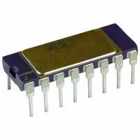
IC AMP INST 1MHZ PREC LN 16CDIP
Manufacturer
Analog Devices Inc
Datasheet
1.AD524ARZ-16.pdf
(28 pages)
Specifications of AD524SD
Rohs Status
RoHS non-compliant
Amplifier Type
Instrumentation
Number Of Circuits
1
Slew Rate
5 V/µs
Gain Bandwidth Product
1MHz
-3db Bandwidth
1MHz
Current - Input Bias
50nA
Voltage - Input Offset
100µV
Current - Supply
3.5mA
Voltage - Supply, Single/dual (±)
±6 V ~ 18 V
Operating Temperature
-55°C ~ 125°C
Mounting Type
Through Hole
Package / Case
16-CDIP (0.300", 7.62mm)
No. Of Amplifiers
1
Input Offset Voltage
100µV
Bandwidth
25MHz
Amplifier Output
Single Ended
Cmrr
110dB
Supply Voltage Range
± 6V To ± 18V
Supply Current
3.5mA
Rohs Compliant
No
Output Type
-
Current - Output / Channel
-
Available stocks
Company
Part Number
Manufacturer
Quantity
Price

Part Number:
AD524SD
Manufacturer:
ADI/亚德诺
Quantity:
20 000
Company:
Part Number:
AD524SD/883B
Manufacturer:
ADI
Quantity:
835


Parameter
TEMPERATURE RANGE
POWER SUPPLY
1
2
@ V
All min and max specifications are guaranteed. Specifications shown in boldface are tested on all production units at the final electrical
test. Results from those tests are used to calculate outgoing quality levels.
Table 2.
Parameter
GAIN
VOLTAGE OFFSET (May be Nulled)
Does not include effects of external resistor, R
V
V
V
Example: G = 10, V
V
OL
DL
D
CM
Specified Performance
Storage
Power Supply Range
Quiescent Current
Gain Equation (External Resistor Gain Programming)
Gain Range (Pin Programmable)
Gain Error
Nonlinearity
Gain vs. Temperature
Input Offset Voltage
Output Offset Voltage
Offset Referred to the Input vs. Supply
= actual differential input voltage.
is the maximum differential input voltage at G = 1 for specified nonlinearity.
at the maximum = 10 V/G.
= 12 V − (10/2 × 0.50 V) = 9.5 V.
S
G = 1
G = 10
G = 100
G = 1000
G = 1
G = 10, G = 100
G = 1000
G = 1
G = 10
G = 100
G = 1000
vs. Temperature
vs. Temperature
= ±15 V, R
G = 1
G = 10
G = 100
G = 1000
1
L
D
= 0.50.
= 2 kΩ and T
A
= +25°C, unless otherwise noted.
G
.
Rev. F | Page 5 of 28
Min
–25
–65
±6
Min
80
100
110
115
⎡
⎢
⎣
40
R
,
000
G
Typ
1 to 1000
AD524A
AD524C
Typ
±15
3.5
+
1
⎤
⎥
⎦
±
Max
±0.02
±0.1
±0.25
±0.5
±0.003
±0.003
±0.01
5
10
25
50
50
0.5
2.0
25
Max
+85
+150
±18
5.0
20
%
Min
–25
–65
±6
Min
75
95
105
110
⎡
⎢
⎣
40
R
,
000
G
Typ
±15
3.5
1 to 1000
Typ
AD524B
AD524S
+
1
⎤
⎥
⎦
±
Max
+85
+150
±18
5.0
Max
±0.05
±0.25
±0.5
±2.0
±0.01
±0.01
±0.01
5
10
25
50
100
2.0
3.0
50
20
%
Unit
°C
°C
V
mA
Unit
%
%
%
%
%
%
%
ppm/°C
ppm/°C
ppm/°C
ppm/°C
μV
μV/°C
mV
μV
dB
dB
dB
dB
AD524
Related parts for AD524SD
Image
Part Number
Description
Manufacturer
Datasheet
Request
R

Part Number:
Description:
±1.7g Dual-Axis IMEMS Accelerometer Evaluation Board
Manufacturer:
Analog Devices Inc
Datasheet:

Part Number:
Description:
Inertial Sensor Evaluation System
Manufacturer:
Analog Devices Inc
Datasheet:
Part Number:
Description:
Manufacturer:
Analog Devices Inc
Datasheet:
Part Number:
Description:
Manufacturer:
Analog Devices Inc
Datasheet:
Part Number:
Description:
Manufacturer:
Analog Devices Inc
Datasheet:
Part Number:
Description:
Manufacturer:
Analog Devices Inc
Datasheet:
Part Number:
Description:
Manufacturer:
Analog Devices Inc
Datasheet:
Part Number:
Description:
Manufacturer:
Analog Devices Inc
Datasheet:
Part Number:
Description:
Manufacturer:
Analog Devices Inc
Datasheet:
Part Number:
Description:
Manufacturer:
Analog Devices Inc
Datasheet:
Part Number:
Description:
Manufacturer:
Analog Devices Inc
Datasheet:
Part Number:
Description:
Manufacturer:
Analog Devices Inc
Datasheet:
Part Number:
Description:
Manufacturer:
Analog Devices Inc
Datasheet: