AD524CD Analog Devices Inc, AD524CD Datasheet
AD524CD
Specifications of AD524CD
Available stocks


Related parts for AD524CD


AD524CD Summary of contents
Page 1
FEATURES Low Noise: 0.3 V p-p 0 Low Nonlinearity: 0.003 High CMRR: 120 1000) Low Offset Voltage Low Offset Voltage Drift: 0 Gain Bandwidth Product: ...
Page 2
AD524–SPECIFICATIONS Model Min GAIN Gain Equation 40 , 000 (External Resistor Gain Programming) Gain Range (Pin Programmable) 1 Gain Error 100 G = 1000 Nonlinearity 10,100 G ...
Page 3
AD524A Model Min Typ SENSE INPUT Voltage Range 10 Gain to Output l REFERENCE INPUT Voltage Range 10 Gain to Output l TEMPERATURE RANGE Specified Performance –25 Storage ...
Page 4
... C to +85 C AD524AE – +85 C AD524AR-16 – +85 C AD524AR-16-REEL – +85 C AD524AR-16-REEL7 – +85 C AD524BD – +85 C AD524BE – +85 C AD524CD – +85 C AD524SD – +125 C AD524SD/883B – +125 C 5962-8853901EA* – +125 C AD524SE/883B – +125 C AD524SCHIPS – +125 C * Refer to official DESC drawing for tested specifications. ...
Page 5
SUPPLY VOLTAGE – V Figure 1. Input Voltage Range vs. Supply Voltage 8.0 6.0 4.0 2 SUPPLY VOLTAGE – ...
Page 6
AD524 –140 G = 1000 G = 100 –120 –100 –80 –60 –40 – 100 1k 10k 100k 1M 10M FREQUENCY – Hz Figure 10. CMRR vs. Frequency RTI, Zero to ...
Page 7
TO +12 1% 0.1% 0.01% – – OUTPUT STEP – – –8 1% 0.1% 0.01% +12 TO – SETTLING TIME – s Figure 19. Settling Time ...
Page 8
AD524 INPUT 100k 20V p-p 0. 100 11k 100 1000 0.1% 0.1% 0. Figure 27. Settling Time Test Circuit + ...
Page 9
Voltage offset and drift comprise two components each; input and output offset and offset drift. Input offset is that component of offset that is directly proportional to gain i.e., input offset as measured at the output 100 ...
Page 10
AD524 Table I. Output Gain Resistor Values Output Gain 1. 4.42 k INPUT BIAS CURRENTS Input bias currents are those currents necessary to bias the ...
Page 11
Separate ground returns should be provided to minimize the current flow in the path from the sensi- tive points to the system ground point. In this way supply currents and logic-gate return currents are not summed into the ...
Page 12
AD524 –IN 1 PROTECTION 2 +IN PROTECTION 3 INPUT OFFSET 4 TRIM R1 10k 5 20k 6 – 35V K1 – ANALOG THERMOSEN DM2C COMMON 4.5V COIL D1 – ...
Page 13
PROTECTION 1 (–INPUT) 4.44k AD524 404 G = 100 1000 11 20k 20k 20k 20k –INPUT 2 PROTECTION (+INPUT ...
Page 14
... The operating temperature range is – +85 C. Therefore, the largest change in temperature T within the operating range is from ambient to +85 C (85 C – C). +10V 350 350 Table II. Error Budget Analysis of AD524CD in Bridge Application AD524C Error Source Specifications Calculation Gain Error 0.25% Gain Instability ...
Page 15
Figure 47 shows a simple application, in which the variation of the cold-junction voltage of a Type J thermocouple-iron(+)– constantan–is compensated for by a voltage developed in series by the temperature-sensitive output current of an AD590 semi- conductor temperature sensor. ...
Page 16
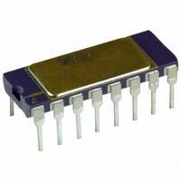
AD524 0.0118 (0.30) 0.0040 (0.10) OUTLINE DIMENSIONS Dimensions shown in inches and (mm). 16-Lead Ceramic DIP (D-16) 0.005 (0.13) MIN 0.080 (2.03) MAX 16 9 0.310 (7.87) 0.220 (5.59 PIN 1 0.060 (1.52) 0.840 (21.34) MAX 0.015 (0.38) ...