AD524CD Analog Devices Inc, AD524CD Datasheet - Page 15
AD524CD
Manufacturer Part Number
AD524CD
Description
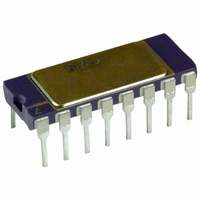
IC AMP INST 1MHZ PREC LN 16CDIP
Manufacturer
Analog Devices Inc
Type
Precisionr
Specifications of AD524CD
Slew Rate
5 V/µs
Rohs Status
RoHS non-compliant
Amplifier Type
Instrumentation
Number Of Circuits
1
Gain Bandwidth Product
1MHz
-3db Bandwidth
1MHz
Current - Input Bias
15nA
Voltage - Input Offset
50µV
Current - Supply
3.5mA
Voltage - Supply, Single/dual (±)
±6 V ~ 18 V
Operating Temperature
-25°C ~ 85°C
Mounting Type
Through Hole
Package / Case
16-CDIP (0.300", 7.62mm)
No. Of Amplifiers
1
Input Offset Voltage
50µV
Gain Db Min
1dB
Gain Db Max
1000dB
Bandwidth
25MHz
Amplifier Output
Single Ended
Cmrr
120dB
Supply Voltage Range
± 6V To ±
Common Mode Rejection Ratio
120
Current, Input Bias
±16 nA
Current, Input Offset
±10 nA
Current, Supply
3.5 mA (Quiescent)
Package Type
SBDIP-16
Power Dissipation
450 mW
Resistance, Input
20 Kilohms
Temperature, Operating, Maximum
85 °C
Temperature, Operating, Minimum
-25 °C
Temperature, Operating, Range
-25 to +85 °C
Voltage, Gain
1-1000 V/V
Voltage, Input
<36 V
Voltage, Input Offset
50 μV
Voltage, Noise
7 nV/sqrt Hz (Input), 90 nV/sqrt Hz (Output)
Voltage, Offset, Input
50 μV (Max.)
Voltage, Supply
±15 V
Output Type
-
Current - Output / Channel
-
Lead Free Status / RoHS Status
Contains lead / RoHS non-compliant
Available stocks
Company
Part Number
Manufacturer
Quantity
Price

Part Number:
AD524CD
Manufacturer:
ADI/亚德诺
Quantity:
20 000


THEORY OF OPERATION
The AD524 is a monolithic instrumentation amplifier based
on the classic 3-op amp circuit. The advantage of monolithic
construction is the closely matched components that enhance
the performance of the input preamplifier. The preamplifier
section develops the programmed gain by the use of feedback
concepts. The programmed gain is developed by varying the
value of R
forces the collector currents (Q1, Q2, Q3, and Q4) to be constant,
which impresses the input voltage across R
As R
transconductance of the input preamplifier increases to the
transconductance of the input transistors. This has three
important advantages. First, this approach allows the circuit
to achieve a very high open-loop gain of 3 × 10
gain of 1000, thus reducing gain-related errors to a negligible
30 ppm. Second, the gain bandwidth product, which is deter-
mined by C3 or C4 and the input transconductance, reaches
25 MHz. Third, the input voltage noise reduces to a value
determined by the collector current of the input transistors
for an RTI noise of 7 nV/√Hz at G = 1000.
INPUT PROTECTION
As interface amplifiers for data acquisition systems, instru-
mentation amplifiers are often subjected to input overloads,
that is, voltage levels in excess of the full scale for the selected
gain range. At low gains (10 or less), the gain resistor acts as a
current limiting element in series with the inputs. At high gains,
the lower value of R
G
is reduced to increase the programmed gain, the
G
(smaller values increase the gain) while the feedback
G
does not adequately protect the inputs
1000
RG
100
10
2
16
13
12
11
1
3
2
–
+
AD524
G
–V
+V
.
7
8
S
8
S
at a programmed
10
6
G = 1000
9
1µF
Figure 33. Noise Test Circuit
16.2kΩ
Rev. F | Page 15 of 28
100Ω
G = 1, 10, 100
3
2
1/2
+
–
+V s
8
1
from excessive currents. Standard practice is to place series
limiting resistors in each input, but to limit input current to
below 5 mA with a full differential overload (36 V) requires
over 7kΩ of resistance, which adds 10 nV√Hz of noise. To
provide both input protection and low noise, a special series
protection FET is used.
A unique FET design was used to provide a bidirectional
current limit, thereby protecting against both positive and
negative overloads. Under nonoverload conditions, three
channels (CH
with the input as before. During an overload in the positive
direction, a fourth channel, CH
(≈3 kΩ) in series with the gate, which draws only the leakage
current, and the FET limits I
a negative overload, the gate current must go through the small
FET formed by CH
the gate current is limited and the main FET goes into controlled
enhancement. The bidirectional limiting holds the maximum
input current to 3 mA over the 36 V range.
INPUT OFFSET AND OUTPUT OFFSET
Voltage offset specifications are often considered a figure of
merit for instrumentation amplifiers. While initial offset may
be adjusted to zero, shifts in offset voltage due to temperature
variations causes errors. Intelligent systems can often correct
this factor with an autozero cycle, but there are many small-
signal high-gain applications that do not have this capability.
AD712
9.09kΩ
1kΩ
1µF
1.62MΩ
5
6
2
, CH
1/2
+
–
–V
4
S
3
1
, CH
and when this FET goes into saturation,
7
4
1µF
) act as a resistance (≈1 kΩ) in series
DSS
16.2kΩ
1.82kΩ
. When the FET enhances under
1
, acts as a small resistance
AD524
Related parts for AD524CD
Image
Part Number
Description
Manufacturer
Datasheet
Request
R

Part Number:
Description:
±1.7g Dual-Axis IMEMS Accelerometer Evaluation Board
Manufacturer:
Analog Devices Inc
Datasheet:

Part Number:
Description:
Inertial Sensor Evaluation System
Manufacturer:
Analog Devices Inc
Datasheet:
Part Number:
Description:
Manufacturer:
Analog Devices Inc
Datasheet:
Part Number:
Description:
Manufacturer:
Analog Devices Inc
Datasheet:
Part Number:
Description:
Manufacturer:
Analog Devices Inc
Datasheet:
Part Number:
Description:
Manufacturer:
Analog Devices Inc
Datasheet:
Part Number:
Description:
Manufacturer:
Analog Devices Inc
Datasheet:
Part Number:
Description:
Manufacturer:
Analog Devices Inc
Datasheet:
Part Number:
Description:
Manufacturer:
Analog Devices Inc
Datasheet:
Part Number:
Description:
Manufacturer:
Analog Devices Inc
Datasheet:
Part Number:
Description:
Manufacturer:
Analog Devices Inc
Datasheet:
Part Number:
Description:
Manufacturer:
Analog Devices Inc
Datasheet:
Part Number:
Description:
Manufacturer:
Analog Devices Inc
Datasheet: