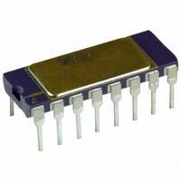
AD524CD Analog Devices Inc, AD524CD Datasheet - Page 16

AD524CD
Manufacturer Part Number
AD524CD
Description
IC AMP INST 1MHZ PREC LN 16CDIP
Manufacturer
Analog Devices Inc
Type
Precisionr
Specifications of AD524CD
Slew Rate
5 V/µs
Rohs Status
RoHS non-compliant
Amplifier Type
Instrumentation
Number Of Circuits
1
Gain Bandwidth Product
1MHz
-3db Bandwidth
1MHz
Current - Input Bias
15nA
Voltage - Input Offset
50µV
Current - Supply
3.5mA
Voltage - Supply, Single/dual (±)
±6 V ~ 18 V
Operating Temperature
-25°C ~ 85°C
Mounting Type
Through Hole
Package / Case
16-CDIP (0.300", 7.62mm)
No. Of Amplifiers
1
Input Offset Voltage
50µV
Gain Db Min
1dB
Gain Db Max
1000dB
Bandwidth
25MHz
Amplifier Output
Single Ended
Cmrr
120dB
Supply Voltage Range
± 6V To ±
Common Mode Rejection Ratio
120
Current, Input Bias
±16 nA
Current, Input Offset
±10 nA
Current, Supply
3.5 mA (Quiescent)
Package Type
SBDIP-16
Power Dissipation
450 mW
Resistance, Input
20 Kilohms
Temperature, Operating, Maximum
85 °C
Temperature, Operating, Minimum
-25 °C
Temperature, Operating, Range
-25 to +85 °C
Voltage, Gain
1-1000 V/V
Voltage, Input
<36 V
Voltage, Input Offset
50 μV
Voltage, Noise
7 nV/sqrt Hz (Input), 90 nV/sqrt Hz (Output)
Voltage, Offset, Input
50 μV (Max.)
Voltage, Supply
±15 V
Output Type
-
Current - Output / Channel
-
Lead Free Status / RoHS Status
Contains lead / RoHS non-compliant
Available stocks
Company
Part Number
Manufacturer
Quantity
Price
Part Number:
AD524CD
Manufacturer:
ADI/亚德诺
Quantity:
20 000
Voltage offset and drift comprise two components each; input
and output offset and offset drift. Input offset is the component
of offset that is directly proportional to gain, that is, input offset
as measured at the output at G = 100 is 100 times greater than at
G = 1. Output offset is independent of gain. At low gains, output
offset drift is dominant, at high gains, input offset drift dominates.
Therefore, the output offset voltage drift is normally specified as
drift at G = 1 (where input effects are insignificant), whereas
input offset voltage drift is given by drift specification at a high
gain (where output offset effects are negligible). All input
related numbers are referred to the input (RTI) that is the effect
on the output is G times larger. Voltage offset vs. power supply
is also specified at one or more gain settings and is also RTI.
By separating these errors, one can evaluate the total error
independent of the gain setting used. In a given gain configura-
tion, both errors can be combined to give a total error referred
to the input (RTI) or output (RTO) by the following formulas:
As an illustration, a typical AD524 might have a +250 μV
output offset and a −50 μV input offset. In a unity gain
configuration, the total output offset would be 200 μV or
the sum of the two. At a gain of 100, the output offset would
be −4.75 mV or: +250 μV + 100(−50 μV) = −4.75 mV.
The AD524 provides for both input and output offset adjustment.
This simplifies very high precision applications and minimizes
offset voltage changes in switched gain applications. In such
applications, the input offset is adjusted first at the highest
programmed gain, then the output offset is adjusted at G = 1.
GAIN
The AD524 has internal high accuracy pretrimmed resistors
for pin programmable gains of 1, 10, 100, and 1000. One of the
preset gains can be selected by pin strapping the appropriate
gain terminal and RG
AD524
–INPUT
+INPUT
Total error RTI = input error + (output error/gain)
Total error RTO = (gain × input error) + output error
G = 1000
G = 100
Figure 34. Operating Connections for G = 100
RG
G = 10
RG
2
1
2
together (for G = 1, RG
16
13
12
11
1
3
2
+V
8
S
AD524
–V
4
7
S
10kΩ
INPUT
OFFSET
NULL
5
10
6
9
2
is not connected).
V
OUTPUT
SIGNAL
COMMON
OUT
Rev. F | Page 16 of 28
The AD524 can be configured for gains other than those that
are internally preset; there are two methods to do this. The first
method uses just an external resistor connected between
Pin 3 and Pin 16 (see Figure 35), which programs the gain
according to the following formula:
For best results, R
temperature coefficient. An external R
accuracy and gain drift due to the mismatch between it and
the internal thin-film resistors. Gain accuracy is determined
by the tolerance of the external R
of the internal resistors (±20%). Gain drift is determined by the
mismatch of the temperature coefficient of R
ture coefficient of the internal resistors (−50 ppm/°C typical).
The second method uses the internal resistors in parallel with
an external resistor (see Figure 36). This technique minimizes
the gain adjustment range and reduces the effects of tempera-
ture coefficient sensitivity.
+INPUT
–INPUT
1.5kΩ
1kΩ
–INPUT
+INPUT
R
G
*R|
*R|
*R|
4kΩ
RG
RG
*NOMINAL (±20%)
=
G = 10
G = 100
G = 1000
Figure 36. Operating Connections for G = 20, Low Gain
1
2
G
40
=
G = 10
2.105kΩ
= 4444.44Ω
k
Figure 35. Operating Connections for G = 20
= 404.04Ω
−
Ω
= 40.04Ω
1
RG
RG
Temperature Coefficient Technique
G
1
2
should be a precision resistor with a low
16
13
12
11
1
3
2
16
13
12
11
1
3
2
AD524
AD524
+V
–V
8
7
S
S
–V
G
+V
8
7
and the absolute accuracy
S
S
G =
G
4000||4444.44
G =
affects both gain
10
6
40,000
10
40,000
6
2.105
9
G
9
and the tempera-
+ 1 = 20 ±20%
+ 1 = 20 ±17%
REFERENCE
V
OUT
V
REFERENCE
OUT


