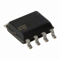
LM2904WHD STMicroelectronics, LM2904WHD Datasheet

LM2904WHD
Specifications of LM2904WHD
Available stocks
Related parts for LM2904WHD
LM2904WHD Summary of contents
Page 1
Features ■ Internally frequency compensated ■ Large DC voltage gain: 100 dB ■ Wide bandwidth (unity gain: 1.1 MHz temperature compensated) ■ Very low supply current per operator (500 µA) ■ Low input bias current (temperaturecompensated) ■ Low ...
Page 2
Schematic diagram 1 Schematic diagram Figure 1. Schematic diagram (1/2 LM2904WH) Figure 2. Pad locations E+ (2) E- (2) y OUT 2 x 2/12 GND E+ (1) E- (1) Vcc + OUT 1 The origin coordinate is at the bottom ...
Page 3
LM2904WH 2 Absolute maximum ratings and operating conditions Table 1. Absolute maximum ratings Symbol + V Supply voltage CC V Differential input voltage id V Input voltage in Output short-circuit to ground T Maximum junction temperature j Thermal resistance junction ...
Page 4
Electrical characteristics 3 Electrical characteristics Table specified) Symbol Input offset voltage V io ≤ min Input offset current I io ≤ min Input bias current I ib ≤ min Large signal ...
Page 5
LM2904WH Table specified) (continued) Symbol Slew rate (unity gain ≤ min Gain bandwidth product f = 100kHz + GBP V CC ≤ min Total harmonic distortion THD f = ...
Page 6
Electrical characteristics Figure 3. Open loop frequency response 120 T =+25°C Ambient 100 T Ambient 80 T =+150°C 60 Ambient FREQUENCY (Hz) Figure 5. Voltage follower pulse response 4 ...
Page 7
LM2904WH Figure 9. Output characteristics 10 VCC = +5V VCC = +15V VCC = +30V 0.1 0.01 0,001 0,01 0,1 OUTPUT SINK CURRENT (μ A) Figure 11. Voltage follower pulse response Figure 13. ...
Page 8
Electrical characteristics Figure 15. Power supply rejection ratio versus temperature P 8/12 Figure 16. Common mode rejection ratio V LM2904WH versus temperature P ...
Page 9
... JEDEC Standard JESD97. The maximum ratings related to soldering conditions are also marked on the inner box label. ECOPACK is an STMicroelectronics trademark. ECOPACK specifications are available at: www.st.com. Package information ...
Page 10
Package information Figure 17. SO-8 package mechanical drawing Table 4. SO-8 package mechanical data Ref ccc 10/12 Dimensions Millimeters Min. Typ. Max. 1.75 0.10 0.25 1.25 0.28 0.48 ...
Page 11
... LM2904WH 5 Ordering information Table 5. Order codes Order code JLM2904WH-CD1 LM2904WHD LM2904WHDT (1) LM2904WHYD (1) LM2904WHYDT 1. Qualified and characterized according to AEC Q100 and Q003 or equivalent, advanced screening according to AEC Q001 & Q 002 or equivalent. 6 Revision history Table 6. Document revision history Date 01-Sep-2003 01-Jul-2005 01-Oct-2005 27-Sep- 2006 ...
Page 12
... Information in this document is provided solely in connection with ST products. STMicroelectronics NV and its subsidiaries (“ST”) reserve the right to make changes, corrections, modifications or improvements, to this document, and the products and services described herein at any time, without notice. All ST products are sold pursuant to ST’s terms and conditions of sale. ...


