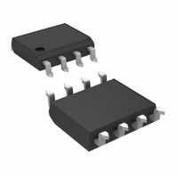
LMP7701MAX/NOPB National Semiconductor, LMP7701MAX/NOPB Datasheet - Page 16

LMP7701MAX/NOPB
Manufacturer Part Number
LMP7701MAX/NOPB
Description
IC OP AMP PREC RRIO SGL 8-SOIC
Manufacturer
National Semiconductor
Series
LMP®r
Datasheet
1.LMP7701MFNOPB.pdf
(24 pages)
Specifications of LMP7701MAX/NOPB
Amplifier Type
General Purpose
Number Of Circuits
1
Output Type
Rail-to-Rail
Slew Rate
1.1 V/µs
Gain Bandwidth Product
2.5MHz
Current - Input Bias
0.2pA
Voltage - Input Offset
37µV
Current - Supply
790µA
Current - Output / Channel
86mA
Voltage - Supply, Single/dual (±)
2.7 V ~ 12 V, ±1.35 V ~ 6 V
Operating Temperature
-40°C ~ 125°C
Mounting Type
Surface Mount
Package / Case
8-SOIC (3.9mm Width)
Lead Free Status / RoHS Status
Lead free / RoHS Compliant
-3db Bandwidth
-
Other names
LMP7701MAX
www.national.com
This equation is rearranged to find the location of the two
poles:
As shown in Equation 1, as values of R
the magnitude of the poles is reduced, which in turn decreas-
es the bandwidth of the amplifier. Whenever possible, it is
best to choose smaller feedback resistors. Figure 3 shows the
effect of the feedback resistor on the bandwidth of the
LMP7701/LMP7702/LMP7704.
Equation 1 has two poles. In most cases, it is the presence of
pairs of poles that causes gain peaking. In order to eliminate
this effect, the poles should be placed in Butterworth position,
since poles in Butterworth position do not cause gain peaking.
To achieve a Butterworth pair, the quantity under the square
root in Equation 1 should be set to equal −1. Using this fact
and the relation between R
value for R
is chosen to be larger than this optimum value, gain peaking
will occur.
In Figure 2, C
and to increase stability. Additionally, C
FIGURE 3. Closed Loop Gain vs. Frequency
1
can be found. This is shown in Equation 2. If R
F
is added to compensate for input capacitance
1
and R
2
, R
2
1
= −A
and R
F
V
reduces or elimi-
R
2
1
are increased,
, the optimum
20127354
(1)
(2)
1
16
nates the gain peaking that can be caused by having a larger
feedback resistor. Figure 4 shows how C
ing.
DIODES BETWEEN THE INPUTS
The LMP7701/LMP7702/LMP7704 have a set of anti-parallel
diodes between the input pins, as shown in Figure 5. These
diodes are present to protect the input stage of the amplifier.
At the same time, they limit the amount of differential input
voltage that is allowed on the input pins. A differential signal
larger than one diode voltage drop might damage the diodes.
The differential signal between the inputs needs to be limited
to ±300 mV or the input current needs to be limited to ±10 mA.
FIGURE 4. Closed Loop Gain vs. Frequency with
FIGURE 5. Input of LMP7701
Compensation
F
reduces gain peak-
20127355
20127325


