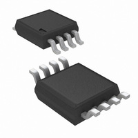
LMP7716MMX/NOPB National Semiconductor, LMP7716MMX/NOPB Datasheet - Page 14

LMP7716MMX/NOPB
Manufacturer Part Number
LMP7716MMX/NOPB
Description
IC AMP PREC 17MHZ DUAL 8-MSOP
Manufacturer
National Semiconductor
Series
LMP®, PowerWise®r
Datasheet
1.LMP7715MFNOPB.pdf
(18 pages)
Specifications of LMP7716MMX/NOPB
Amplifier Type
General Purpose
Number Of Circuits
2
Output Type
Rail-to-Rail
Slew Rate
11.5 V/µs
Gain Bandwidth Product
17MHz
Current - Input Bias
0.1pA
Voltage - Input Offset
10µV
Current - Supply
1.3mA
Current - Output / Channel
66mA
Voltage - Supply, Single/dual (±)
1.8 V ~ 5.5 V
Operating Temperature
-40°C ~ 125°C
Mounting Type
Surface Mount
Package / Case
8-MSOP, Micro8™, 8-uMAX, 8-uSOP,
Lead Free Status / RoHS Status
Lead free / RoHS Compliant
-3db Bandwidth
-
Other names
LMP7716MMX
Available stocks
Company
Part Number
Manufacturer
Quantity
Price
Company:
Part Number:
LMP7716MMX/NOPB
Manufacturer:
TI
Quantity:
1 560
www.national.com
Application Information
LMP7715/LMP7716/LMP7716Q
The LMP7715/LMP7716/LMP7716Q are single and dual, low
noise, low offset, rail-to-rail output precision amplifiers with a
wide gain bandwidth product of 17 MHz and low supply cur-
rent. The wide bandwidth makes the LMP7715/LMP7716/
LMP7716Q ideal choices for wide-band amplification in
portable applications.
The LMP7715/LMP7716/LMP7716Q are superior for sensor
applications. The very low input referred voltage noise of only
5.8 nV/
of only 10 fA/
to-noise ratio.
The LMP7715/LMP7716/LMP7716Q have a supply voltage
range of 1.8V to 5.5V over a wide temperature range of 0°C
to 125°C. This is optimal for low voltage commercial applica-
tions. For applications where the ambient temperature might
be less than 0°C, the LMP7715/LMP7716/LMP7716Q are ful-
ly operational at supply voltages of 2.0V to 5.5V over the
temperature range of −40°C to 125°C.
The outputs of the LMP7715/LMP7716/LMP7716Q swing
within 25 mV of either rail providing maximum dynamic range
in applications requiring low supply voltage. The input com-
mon mode range of the LMP7715/LMP7716/LMP7716Q ex-
tends to 300 mV below ground. This feature enables users to
utilize this device in single supply applications.
The use of a very innovative feedback topology has enhanced
the current drive capability of the LMP7715/LMP7716/LM-
P7716Q, resulting in sourcing currents of as much as 47 mA
with a supply voltage of only 1.8V.
The LMP7715 is offered in the space saving SOT-23 package
and the LMP7716/LMP7716Q is offered in an 8-pin MSOP.
These small packages are ideal solutions for applications re-
quiring minimum PC board footprint.
CAPACITIVE LOAD
The unity gain follower is the most sensitive configuration to
capacitive loading. The combination of a capacitive load
placed directly on the output of an amplifier along with the
output impedance of the amplifier creates a phase lag which
in turn reduces the phase margin of the amplifier. If phase
margin is significantly reduced, the response will be either
underdamped or the amplifier will oscillate.
The LMP7715/LMP7716/LMP7716Q can directly drive ca-
pacitive loads of up to 120 pF without oscillating. To drive
heavier capacitive loads, an isolation resistor, R
in
and hence delay the phase lag or increase the phase margin
of the overall system. The larger the value of R
stable the output voltage will be. However, larger values of
R
rent drive.
ISO
Figure
result in reduced output swing and reduced output cur-
1, should be used. This resistor and C
FIGURE 1. Isolating Capacitive Load
at 1 kHz and very low input referred current noise
mean more signal fidelity and higher signal-
20183661
ISO
ISO
L
form a pole
, the more
as shown
14
INPUT CAPACITANCE
CMOS input stages inherently have low input bias current and
higher input referred voltage noise. The LMP7715/LMP7716/
LMP7716Q enhance this performance by having the low input
bias current of only 50 fA, as well as, a very low input referred
voltage noise of 5.8 nV/
input stage has been used. This larger input stage increases
the input capacitance of the LMP7715/LMP7716/LMP7716Q.
Figure 2
the LMP7715/LMP7716/LMP7716Q.
This input capacitance will interact with other impedances,
such as gain and feedback resistors which are seen on the
inputs of the amplifier, to form a pole. This pole will have little
or no effect on the output of the amplifier at low frequencies
and under DC conditions, but will play a bigger role as the
frequency increases. At higher frequencies, the presence of
this pole will decrease phase margin and also cause gain
peaking. In order to compensate for the input capacitance,
care must be taken in choosing feedback resistors. In addition
to being selective in picking values for the feedback resistor,
a capacitor can be added to the feedback path to increase
stability.
The DC gain of the circuit shown in
R
1
.
FIGURE 3. Compensating for Input Capacitance
FIGURE 2. Input Common Mode Capacitance
shows typical input common mode capacitance of
. In order to achieve this a larger
Figure 3
20183664
is simply −R
20183675
2
/


