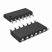
LF347M/NOPB National Semiconductor, LF347M/NOPB Datasheet

LF347M/NOPB
Specifications of LF347M/NOPB
*LF347M/NOPB
LF347M
Available stocks
Related parts for LF347M/NOPB
LF347M/NOPB Summary of contents
Page 1
... The device has low noise and offset voltage drift. Simplified Schematic 1 ⁄ Quad 4 BI-FET II ™ trademark of National Semiconductor Corporation. © 2004 National Semiconductor Corporation Features n Internally trimmed offset voltage: n Low input bias current: n Low input noise current: n Wide gain bandwidth: n High slew rate: n Low supply current: ...
Page 2
... Absolute Maximum Ratings If Military/Aerospace specified devices are required, please contact the National Semiconductor Sales Office/ Distributors for availability and specifications. LF147 ± Supply Voltage ± Differential Input Voltage ± Input Voltage Range (Note 3) Output Short Circuit Continuous Duration (Note 4) Power Dissipation ...
Page 3
AC Electrical Characteristics Symbol Parameter Amplifier to Amplifier Coupling SR Slew Rate GBW Gain-Bandwidth Product e Equivalent Input Noise Voltage n i Equivalent Input Noise Current n THD Total Harmonic Distortion Note 2: Absolute Maximum Ratings indicate limits beyond which ...
Page 4
Typical Performance Characteristics Input Bias Current Supply Current Negative Common-Mode Input Voltage Limit www.national.com 00564714 Positive Common-Mode 00564716 Positive Current Limit 00564718 4 Input Bias Current 00564715 Input Voltage Limit 00564717 00564719 ...
Page 5
Typical Performance Characteristics Negative Current Limit Output Voltage Swing Bode Plot (Continued) Output Voltage Swing 00564720 00564722 00564724 5 00564721 Gain Bandwidth 00564723 Slew Rate 00564725 www.national.com ...
Page 6
Typical Performance Characteristics Distortion vs Frequency Open Loop Frequency Response Power Supply Rejection Ratio www.national.com (Continued) Undistorted Output Voltage 00564726 Common-Mode Rejection 00564728 Equivalent Input Noise 00564730 6 Swing 00564727 Ratio 00564729 Voltage 00564731 ...
Page 7
Typical Performance Characteristics Open Loop Voltage Gain Inverter Settling Time (Continued) Output Impedance 00564732 00564734 7 00564733 www.national.com ...
Page 8
Pulse Response R =2 kΩ Small Signal Inverting Small Signal Non-Inverting Application Hints The LF147 amp with an internally trimmed input offset voltage and JFET input devices (BI-FET II). These JFETs have large reverse breakdown ...
Page 9
Application Hints (Continued) Exceeding the positive common-mode limit on a single input will not change the phase of the output; however, if both inputs exceed the limit, the output of the amplifier will be forced to a high state. The ...
Page 10
Typical Applications All resistors 1% tolerance • Accuracy of better than 0.4% with standard 1% value resistors No offset adjustment necessary • Expandable to any number of stages • Very high input impedance www.national.com Digitally Selectable Precision Attenuator A1 A2 ...
Page 11
Typical Applications (Continued) Long Time Integrator with Reset, Hold and Starting Threshold Adjustment • V starts from zero and is equal to the integral of the input voltage with respect to the threshold voltage: OUT ≥V • Output starts when ...
Page 12
Typical Applications For circuit shown kHz, f =9.5 kHz o NOTCH Q=3.4 Passband gain: Highpass — 0.1 Bandpass — 1 Lowpass — 1 Notch — 10 • f xQ≤200 kHz o • 10V peak sinusoidal output swing without ...
Page 13
Physical Dimensions inches (millimeters) unless otherwise noted Order Number LF147J, LM147J-SMD or LF147J/883 Ceramic Dual-In-Line Package (J) NS Package Number J14A S.O. Package (M) Order Number LF347M or LF347MX NS Package Number M14A 13 www.national.com ...
Page 14
... BANNED SUBSTANCE COMPLIANCE National Semiconductor certifies that the products and packing materials meet the provisions of the Customer Products Stewardship Specification (CSP-9-111C2) and the Banned Substances and Materials of Interest Specification (CSP-9-111S2) and contain no ‘‘Banned Substances’’ as defined in CSP-9-111S2. ...


