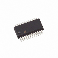
EL5373IUZ-T13 Intersil, EL5373IUZ-T13 Datasheet

EL5373IUZ-T13
Specifications of EL5373IUZ-T13
Related parts for EL5373IUZ-T13
EL5373IUZ-T13 Summary of contents
Page 1
... OUT3 + EL5373IU - 14 OUT3B EL5373IUZ* (Note) EL5373IUZ 13 NC *Add “-T7” or “-T13” suffix for tape and reel. Please refer to TB347 for details on reel specifications. NOTE: These Intersil Pb-free plastic packaged products employ special Pb-free material sets, molding compounds/die attach materials, and 100% matte tin plate plus anneal (e3 termination finish, which is RoHS compliant and compatible with both SnPb and Pb-free soldering operations) ...
Page 2
... EL5173, EL5373 Thermal Information = +25°C) Operating Junction Temperature . . . . . . . . . . . . . . . . . . . . . . +135°C Recommended Operating Temperature . . . . . . . . . .-40°C to +85°C Storage Temperature Range . . . . . . . . . . . . . . . . . .-65°C to +150° 0. 0.3V Power Dissipation . . . . . . . . . . . . . . . . . . . . . . . . . . . . . See Curves S S Pb-Free Reflow Profile .see link below http://www.intersil.com/pbfree/Pb-FreeReflow.asp = -5V +25° 0V CONDITIONS 20% to 80% ...
Page 3
Electrical Specifications +5V PARAMETER DESCRIPTION CMIR- Common Mode Negative Input Range Reference Input - Positive REFIN V - Reference Input - Negative REFIN V Output Offset ...
Page 4
Pin Descriptions EL5173 PIN NUMBER PIN NAME PIN NUMBER REF OUTB 14 OUT 15, ...
Page 5
Connection Diagrams INP INN REF INP1 INN1 REF1 INP2 INN2 REF2 INP3 INN3 REF3 SP1 SN1 SR1 50Ω 50Ω 50Ω 50Ω R -5V S1 50Ω 1 IN+ OUT VS- 7 IN- 3 ...
Page 6
Typical Performance Curves V = ±5V 200Ω ODP 10M FREQUENCY (Hz) FIGURE 3. FREQUENCY RESPONSE V = ±5V 200Ω ...
Page 7
Typical Performance Curves 100Ω ODM R 100Ω 0 -10 -20 -30 - OCM ODM -50 -60 100k 1M 10M FREQUENCY (Hz) FIGURE 9. DIFFERENTIAL MODE OUTPUT BALANCE ERROR vs FREQUENCY -30 ...
Page 8
Typical Performance Curves V = ±5V ODMP-P -40 -50 HD3 (f = 20MHz) -60 -70 HD2 (f = 20MHz) -80 -90 HD2 (f = 5MHz) -100 100 200 300 400 500 600 R (Ω) LD FIGURE ...
Page 9
Typical Performance Curves FIGURE 21. DISABLED RESPONSE JEDEC JESD51-7 HIGH EFFECTIVE THERMAL CONDUCTIVITY TEST BOARD 1.4 1.136W 1.2 QSOP24 1.0 909mW θ = +88°C/W JA 0.8 870mW θ JA 0.6 MSOP8/10 0.4 θ = +115°C ...
Page 10
Description of Operation and Application Information Product Description The EL5173 and EL5373 are wide bandwidth, low power and single/differential ended to differential output amplifiers. They have a fixed gain of 2. The EL5173 is a single channel differential amplifier. The ...
Page 11
By setting the two PD equations equal to each other, we MAX can solve the output current and R LOAD overheat. Power Supply Bypassing and Printed Circuit Board Layout As with any high frequency device, a good printed circuit board ...
Page 12
Package Outline Drawing M8.15E 8 LEAD NARROW BODY SMALL OUTLINE PLASTIC PACKAGE Rev 0, 08/09 4 4.90 ± 0.10 PIN NO.1 ID MARK 5 1.27 TOP VIEW 1.75 MAX 0.175 ± 0.075 SIDE VIEW “A (1.27) (5.40) TYPICAL RECOMMENDED LAND ...
Page 13
Package Outline Drawing M8.118A 8 LEAD MINI SMALL OUTLINE PLASTIC PACKAGE (MSOP) Rev 0, 9/09 3.0±0.1 8 PIN 0.65 BSC TOP VIEW H 0.33 +0.07/ -0.08 0. SIDE VIEW 1 5.80 4.40 3.00 ...
Page 14
... Accordingly, the reader is cautioned to verify that data sheets are current before placing orders. Information furnished by Intersil is believed to be accurate and reliable. However, no responsibility is assumed by Intersil or its subsidiaries for its use; nor for any infringements of patents or other rights of third parties which may result from its use ...


