NCV2001SN2T1G ON Semiconductor, NCV2001SN2T1G Datasheet
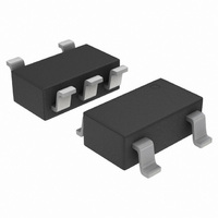
IC OP AMP R-R SGL 0.9V SOT23-5

NCV2001SN2T1G

Manufacturer Part Number
NCV2001SN2T1G
Description
IC OP AMP R-R SGL 0.9V SOT23-5
Manufacturer
ON Semiconductor
Datasheet

Specifications of NCV2001SN2T1G

Amplifier Type
General Purpose
Number Of Circuits
1
Output Type
Rail-to-Rail
Slew Rate
1.6 V/µs
Gain Bandwidth Product
1.4MHz
Current - Input Bias
10pA
Voltage - Input Offset
500µV
Current - Supply
820µA
Current - Output / Channel
96mA
Voltage - Supply, Single/dual (±)
0.9 V ~ 7 V, ±0.45 V ~ 3.5 V
Operating Temperature
-40°C ~ 125°C
Mounting Type
Surface Mount
Package / Case
TSOT-23-5, TSOT-5, TSOP-5
Number Of Channels
1
Voltage Gain Db
92.04 dB
Common Mode Rejection Ratio (min)
60 dB
Input Offset Voltage
6 mV
Operating Supply Voltage
3 V, 5 V
Supply Current
1.5 mA
Maximum Power Dissipation
340 mW
Maximum Operating Temperature
+ 125 C
Mounting Style
SMD/SMT
Maximum Dual Supply Voltage
+/- 3.5 V
Minimum Operating Temperature
- 40 C
Lead Free Status / RoHS Status
Lead free / RoHS Compliant
-3db Bandwidth
-
Lead Free Status / Rohs Status
 Details

Available stocks

Company
Part Number
Manufacturer
Quantity
Price
Part Number:
NCV2001SN2T1G
Manufacturer:
ON/安森美
Quantity:
20 000
NCS2001, NCV2001
0.9 V, Rail−to−Rail, Single
Operational Amplifier
amplifier that features a rail−to−rail common mode input voltage range,
along with rail−to−rail output drive capability. This amplifier is
guaranteed to be fully operational down to 0.9 V, providing an ideal
solution for powering applications from a single cell Nickel Cadmium
(NiCd) or Nickel Metal Hydride (NiMH) battery. Additional features
include no output phase reversal with overdriven inputs, trimmed input
offset voltage of 0.5 mV, extremely low input bias current of 40 pA, and
a unity gain bandwidth of 1.4 MHz at 5.0 V. The tiny NCS2001 is the
ideal solution for small portable electronic applications and is available
in the space saving SOT23−5 and SC70−5 packages with two industry
standard pinouts.
Features
Typical Applications
© Semiconductor Components Industries, LLC, 2007
January, 2007 − Rev. 15
The NCS2001 is an industry first sub−one voltage operational
and Control Changes
0.9 V Guaranteed Operation
Rail−to−Rail Common Mode Input Voltage Range
Rail−to−Rail Output Drive Capability
No Output Phase Reversal for Over−Driven Input Signals
0.5 mV Trimmed Input Offset
10 pA Input Bias Current
1.4 MHz Unity Gain Bandwidth at "2.5 V, 1.1 MHz at "0.5 V
Tiny SC70−5 and SOT23−5 Packages
NCV Prefix for Automotive and Other Applications Requiring Site
Pb−Free Package is Available
Single Cell NiCd/NiMH Battery Powered Applications
Cellular Telephones
Pagers
Personal Digital Assistants
Electronic Games
Digital Cameras
Camcorders
Hand−Held Instruments
0.8 V
7.0 V
to
Rail to Rail Input
This device contains 63 active transistors.
Figure 1. Typical Application
+
Rail to Rail Output
1
See detailed ordering and shipping information in the
dimensions section on page 15 of this data sheet.
Non−Inverting
Non−Inverting
CASE 419A
SN SUFFIX
SQ SUFFIX
CASE 483
5
SOT23−5
5
SC70−5
(Note: Microdot may be in either location)
4
1 2
1
Style 1 Pinout (SN1T1, SQ1T2)
Style 2 Pinout (SN2T1, SQ2T2)
ORDERING INFORMATION
V
V
Input
Input
V
3
V
OUT
OUT
CC
PIN CONNECTIONS
EE
http://onsemi.com
x = G for SN1
A = Assembly Location
Y = Year
W = Work Week
M = Date Code
G = Pb−Free Package
5
1
1
2
3
1
2
3
H for SN2
I for SQ1
J for SQ2
AAx AYWG
MARKING DIAGRAMS
+ −
+ −
Publication Order Number:
G
5
1
5
4
5
4
|
V
Inverting
Input
V
Inverting
Input
5
1
AAx
EE
CC
NCV2001SN2
MBB AYWG
NCS2001/D
G

Related parts for NCV2001SN2T1G

NCV2001SN2T1G Summary of contents

Page 1

NCS2001, NCV2001 0.9 V, Rail−to−Rail, Single Operational Amplifier The NCS2001 is an industry first sub−one voltage operational amplifier that features a rail−to−rail common mode input voltage range, along with rail−to−rail output drive capability. This amplifier is guaranteed to be fully ...

Page 2

MAXIMUM RATINGS Rating Supply Voltage ( Input Differential Voltage Range (Note 1) Input Common Mode Voltage Range (Note 1) Output Short Circuit Duration (Note 2) Junction Temperature Power Dissipation and Thermal Characteristics SOT23−5 Package Thermal ...

Page 3

DC ELECTRICAL CHARACTERISTICS (continued 2 −2 Characteristics Output Voltage Swing, High State Output ( 0. −0. ...

Page 4

DC ELECTRICAL CHARACTERISTICS (continued 2 −2 Characteristics Common Mode Rejection Ratio ( 5 Power Supply Rejection Ratio (V ...

Page 5

V −0 High State Output GND −0.4 Sourcing Current 25°C A −0.6 0.6 0.4 Low State Output Sinking Current 0.2 0 100 1 Load Resistance (W) ...

Page 6

V = ±2 1 25° ±1 ±0 1.E+03 1.E+04 1.E+05 f, Frequency ...

Page 7

A = 1000 V 1 100 V 0 1.0 0. ±0 0.4 V out 0.001 10 100 1 Frequency (Hz) Figure 14. ...

Page 8

V = ±0 ±2 − 25°C A − 100 k 1 Frequency (Hz) Figure 20. Voltage Gain and ...

Page 9

0.0 0.5 1.0 1 Supply Voltage (V) S Figure 26. Open Loop Voltage Gain vs. Supply Voltage ±2 ...

Page 10

APPLICATION INFORMATION AND OPERATING DESCRIPTION GENERAL INFORMATION The NCS2001 is an industry first rail−to−rail input, rail−to−rail output amplifier that features guaranteed sub−one voltage operation. This unique feature set is achieved with the use of a modified analog CMOS process that ...

Page 11

Figure 32. Small Signal Transient Response with Large Capacitive Load Figure 33. Small Signal Transient Response with Large Capacitive Load and Isolation Resistor http://onsemi.com out out ±0. ...

Page 12

R T 470 k 0 1.0 nF − 470 k 0 470 k 470 cww 1 1.0 nF ...

Page 13

Figure 36. Positive Capacitance Multiplier C f 400 100 k 0 − −0 Figure 37. 1.0 ...

Page 14

V in Figure 38. High Compliance Current Sink sense − 3.3 k Figure 39. High Side Current Sense V supply V CC ...

Page 15

... NCS2001SQ1T1G NCS2001SQ1T2 NCS2001SQ1T2G NCS2001SQ2T2 NCS2001SQ2T2G NCV2001SN2T1G* †For information on tape and reel specifications, including part orientation and tape sizes, please refer to our Tape and Reel Packaging Specifications Brochure, BRD8011/D. *NCV prefix denotes qualification status for automotive applications. Guaranteed by design. Package SOT23−5 SOT23− ...

Page 16

... A C SEATING 0.05 PLANE H T *For additional information on our Pb−Free strategy and soldering details, please download the ON Semiconductor Soldering and Mounting Techniques Reference Manual, SOLDERRM/D. PACKAGE DIMENSIONS TSOP−5 CASE 483−02 ISSUE F NOTES: 1. DIMENSIONING AND TOLERANCING PER 2. CONTROLLING DIMENSION: MILLIMETERS. ...

Page 17

... Pb−Free strategy and soldering details, please download the ON Semiconductor Soldering and Mounting Techniques Reference Manual, SOLDERRM/D. ON Semiconductor and are registered trademarks of Semiconductor Components Industries, LLC (SCILLC). SCILLC reserves the right to make changes without further notice to any products herein ...

Related keywords