NCV2002SN2T1G ON Semiconductor, NCV2002SN2T1G Datasheet
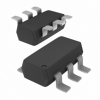
IC OPAMP R-R 0.9V 1A 6-TSOP

NCV2002SN2T1G

Manufacturer Part Number
NCV2002SN2T1G
Description
IC OPAMP R-R 0.9V 1A 6-TSOP
Manufacturer
ON Semiconductor
Datasheet

Specifications of NCV2002SN2T1G

Amplifier Type
General Purpose
Number Of Circuits
1
Output Type
Rail-to-Rail
Slew Rate
1.3 V/µs
Gain Bandwidth Product
900kHz
Current - Input Bias
10pA
Voltage - Input Offset
500µV
Current - Supply
820µA
Current - Output / Channel
128mA
Voltage - Supply, Single/dual (±)
0.9 V ~ 7 V, ±0.45 V ~ 3.5 V
Operating Temperature
-40°C ~ 125°C
Mounting Type
Surface Mount
Package / Case
SC-74-6
Number Of Channels
1
Voltage Gain Db
92.04 dB
Common Mode Rejection Ratio (min)
60 dB
Input Voltage Range (max)
Positive Rail
Input Voltage Range (min)
Negative Rail
Input Offset Voltage
6 mV
Operating Supply Voltage
7 V
Supply Current
2 uA
Maximum Power Dissipation
340 mW
Maximum Operating Temperature
+ 125 C
Mounting Style
SMD/SMT
Maximum Dual Supply Voltage
+/- 3.5 V
Minimum Operating Temperature
- 40 C
Lead Free Status / RoHS Status
Lead free / RoHS Compliant
-3db Bandwidth
-
Lead Free Status / Rohs Status
 Details
Other names
NCV2002SN2T1G
NCV2002SN2T1GOSTR

Available stocks

Company
Part Number
Manufacturer
Quantity
Price
Part Number:
NCV2002SN2T1G
Manufacturer:
ON/安森美
Quantity:
20 000
Part Number:
NCV2002SN2T1G
0
NCS2002, NCV2002
Sub−One Volt Rail−to−Rail
Operational Amplifier with
Enable Feature
that features a rail−to−rail common mode input voltage range, along
with rail−to−rail output drive capability. This amplifier is guaranteed
to be fully operational down to 0.9 V, providing an ideal solution for
powering applications from a single cell Nickel Cadmium (NiCd) or
Nickel Metal Hydride (NiMH) battery. Additional features include no
output phase reversal with overdriven inputs, trimmed input offset
voltage of 0.5 mV, extremely low input bias current of 40 pA, and a
unity gain bandwidth of 1.1 MHz at 5.0 V.
shutdown of the device. In the standby mode, the supply current is
typically 1.9 mA at 1.0 V. Because of its small size and enable feature,
this amplifier represents the ideal solution for small portable
electronic applications. The NCS2002 is available in the space saving
SOT23−6 (TSOP−6) package with two industry standard pinouts.
Features
Typical Applications
© Semiconductor Components Industries, LLC, 2007
January, 2007 − Rev. 6
The NCS2002 is an industry first sub−one volt operational amplifier
The NCS2002 also has an active high enable pin that allows external
0.9 V Guaranteed Operation
Standby Mode: I
Rail−to−Rail Common Mode Input Voltage Range
Rail−to−Rail Output Drive Capability
No Output Phase Reversal for Over−Driven Input Signals
0.5 mV Trimmed Input Offset
10 pA Input Bias Current
1.1 MHz Unity Gain Bandwidth at $2.5 V, 1.0 MHz at $0.5 V
Tiny SOT23−6 (TSOP−6) Package
Pb−Free Packages are Available
Single Cell NiCd / NiMH Battery Powered Applications
Cellular Telephones
Pagers
Personal Digital Assistants
Electronic Games
Digital Cameras
Camcorders
Hand Held Instruments
0.8 V
7.0 V
to
Rail to Rail Input
This device contains 81 active transistors.
Figure 1. Typical Application
D
= 1.9 mA at 1.0 V, Typical
+
Rail to Rail Output
1
See detailed ordering, marking, and shipping information in
the package dimensions section on page 15 of this data sheet.
ORDERING AND MARKING INFORMATION
Non−Inverting
Non−Inverting
AA
x =
A
Y
W
G
(Note: Microdot may be in either location)
= Device Code
Marking Defined on Page 15 in
Ordering Information
= Assembly Location
= Year
= Work Week
= Pb−Free Package
V
V
Input
Input
V
V
OUT
OUT
MARKING DIAGRAM
CC
PIN CONNECTIONS
EE
Style 1 Pinout (SN1T1)
Style 2 Pinout (SN2T1)
http://onsemi.com
1
1
2
3
1
2
3
CASE 318G
SN SUFFIX
AAxAYW G
TSSOP−6
+ −
+ −
Publication Order Number:
G
1
6
5 Enable
4
6
5 Enable
4
V
Inverting
Input
V
Inverting
Input
EE
CC
NCS2002/D

Related parts for NCV2002SN2T1G

NCV2002SN2T1G Summary of contents

Page 1

NCS2002, NCV2002 Sub−One Volt Rail−to−Rail Operational Amplifier with Enable Feature The NCS2002 is an industry first sub−one volt operational amplifier that features a rail−to−rail common mode input voltage range, along with rail−to−rail output drive capability. This amplifier is guaranteed to ...

Page 2

MAXIMUM RATINGS Rating Supply Voltage ( Input Differential Voltage Range (Note 1) Input Common Mode Voltage Range (Note 1) Output Short Circuit Duration (Note 2) Junction Temperature Power Dissipation and Thermal Characteristics SOT23−6 Package Thermal ...

Page 3

DC ELECTRICAL CHARACTERISTICS Rating Output Voltage Swing, Low State Output ( −40 to +125° 0. −0. 2 1.5 ...

Page 4

AC ELECTRICAL CHARACTERISTICS Rating Differential Input Resistance ( Differential Input Capacitance ( Equivalent Input Noise Voltage (f = 1.0 kHz) Gain Bandwidth Product (f = 100 kHz 0. ...

Page 5

V −200 S R High State Output L T −400 Sourcing Current A −600 600 400 Low State Output Sinking Current 200 0 100 1 Load Resistance (W) L Figure 2. Output Saturation Voltage ...

Page 6

V = ±3 6 ±2 4.0 2 ±0. 1 100 k f, Frequency (Hz) Figure 8. Output Voltage versus Frequency 120 100 PSR + ...

Page 7

V = ±0 0.4 V out 2 25°C A 0.01 10 100 1 Frequency (Hz) Figure 14. Total Harmonic Distortion versus Frequency with 1.0 ...

Page 8

V = ±2 ±0 ±2 ±0 100 k L − 25°C A Amp = 0.8 mV −40 10 ...

Page 9

V , Supply Voltage (V) S Figure 26. Open Loop Voltage Gain versus Supply Voltage ±0 ∞ ...

Page 10

Figure 32. Propagation Delay versus Supply Voltage APPLICATION INFORMATION AND OPERATING DESCRIPTION GENERAL INFORMATION The NCS2002 is an industry first rail−to−rail input, rail−to−rail output amplifier that features guaranteed sub one ...

Page 11

Output The output stage consists of complementary P and N channel devices connected to provide rail−to−rail output drive. With a 2.0 k load, the output can swing within either rail also capable of supplying over ...

Page 12

Figure 35. Small Signal Transient Response with Large Capacitive Load Figure 36. Small Signal Transient Response with Large Capacitive Load and Isolation Resistor. http://onsemi.com out out ±0. ...

Page 13

R T 470 k 0 1.0 nF − 470 k 0 470 k 470 cww 1 1.0 nF ...

Page 14

Figure 39. Positive Capacitance Multiplier C f 400 100 k 0 − −0 Figure 40. 1.0 ...

Page 15

... NCS2002SN2T1 NCS2002SN2T1G NCV2002SN1T1 NCV2002SN1T1G NCV2002SN2T1 NCV2002SN2T1G †For information on tape and reel specifications, including part orientation and tape sizes, please refer to our Tape and Reel Packaging Specifications Brochure, BRD8011/D. *NCV2002 −40° +125°C. Guaranteed by design. NCV prefix is for automotive and other applications requiring site and change ...

Page 16

... Pb−Free strategy and soldering details, please download the ON Semiconductor Soldering and Mounting Techniques Reference Manual, SOLDERRM/D. ON Semiconductor and are registered trademarks of Semiconductor Components Industries, LLC (SCILLC). SCILLC reserves the right to make changes without further notice to any products herein ...

Related keywords