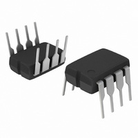
MC33202VPG ON Semiconductor, MC33202VPG Datasheet

MC33202VPG
Specifications of MC33202VPG
Available stocks
Related parts for MC33202VPG
MC33202VPG Summary of contents
Page 1
MC33201, MC33202, MC33204, NCV33202, NCV33204 Low Voltage, Rail-to-Rail Operational Amplifiers The MC33201/2/4 family of operational amplifiers provide rail−to−rail operation on both the input and output. The inputs can be driven as high as 200 mV beyond the supply rails without ...
Page 2
MC33201 All Case Styles Inputs (Top View) MC33202 All Case Styles Output Inputs (Top View ...
Page 3
MAXIMUM RATINGS Rating Supply Voltage ( Input Differential Voltage Range Common Mode Input Voltage Range (Note 2) Output Short Circuit Duration Maximum Junction Temperature Storage Temperature Maximum Power Dissipation DC ELECTRICAL CHARACTERISTICS Characteristic Input Offset ...
Page 4
DC ELECTRICAL CHARACTERISTICS (cont.) Characteristic Input Offset Current ( 0 25° − 40° to +105° − 55° to +125°C A Common Mode Input Voltage ...
Page 5
Pin DIP Pkg 2000 TSSOP-14 Pkg 1500 SO-14 Pkg 1000 SOIC-8 Pkg 500 AMBIENT TEMPERATURE (°C) A Figure 2. Maximum Power Dissipation versus Temperature ...
Page 6
25° 8.0 6.0 4.0 2.0 0 ±1.0 ± 2.0 ± 3.0 ± 4.0 ⎮ SUPPLY VOLTAGE (V) V ,⎮ Figure 8. Output Voltage Swing versus Supply Voltage 12 ...
Page 7
5 Gnd 125 EE 100 Source 75 Sink AMBIENT TEMPERATURE (°C) A Figure 14. Output Short Circuit Current versus ...
Page 8
Phase Margin 6 6 600 100 Gain Margin ...
Page 9
General Information The MC33201/2/4 family of operational amplifiers are unique in their ability to swing rail−to−rail on both the input and the output with a completely bipolar design. This offers low noise, high output current capability and a wide common ...
Page 10
... Dual MC33202VDG MC33202VDR2G NCV33202VDR2* NCV33202VDR2G* MC33202VP MC33202VPG †For information on tape and reel specifications, including part orientation and tape sizes, please refer to our Tape and Reel Packaging Specifications Brochure, BRD8011/D. *NCV33202 and NCV33204 are qualified for automotive use. Operating Package Temperature Range SOIC− ...
Page 11
ORDERING INFORMATION (continued) Operational Device Amplifier Function MC33204DG MC33204DR2G MC33204DTBG MC33204DTBR2G MC33204PG MC33204VD Quad MC33204VDG MC33204VDR2G NCV33204DR2G** NCV33204DTBR2G** MC33204VPG †For information on tape and reel specifications, including part orientation and tape sizes, please refer to our Tape and Reel Packaging ...
Page 12
SOIC−8 SOIC−8 D SUFFIX VD SUFFIX CASE 751 CASE 751 3320x 320xV ALYW ALYW SO−14 PDIP−14 VD SUFFIX P SUFFIX CASE 751A CASE 646 MC33204P MC33204VDG AWLYYWWG AWLYWW 1 1 ...
Page 13
NOTE 5 F TOP VIEW e 0.010 SIDE VIEW PACKAGE DIMENSIONS PDIP− SUFFIX CASE 626−05 ISSUE M NOTES: 1. DIMENSIONING AND TOLERANCING PER ...
Page 14
... G C SEATING PLANE −Z− 0.25 (0.010 *For additional information on our Pb−Free strategy and soldering details, please download the ON Semiconductor Soldering and Mounting Techniques Reference Manual, SOLDERRM/D. PACKAGE DIMENSIONS SOIC−8 NB CASE 751−07 ISSUE 0.10 (0.004 SOLDERING FOOTPRINT* 1 ...
Page 15
... PLANE A 0.038 (0.0015) A1 1.04 8X 0.041 *For additional information on our Pb−Free strategy and soldering details, please download the ON Semiconductor Soldering and Mounting Techniques Reference Manual, SOLDERRM/D. PACKAGE DIMENSIONS Micro8 DM SUFFIX CASE 846A−02 ISSUE H NOTES: 1. DIMENSIONING AND TOLERANCING PER ANSI Y14.5M, 1982. ...
Page 16
−T− SEATING PLANE 0.13 (0.005) PACKAGE DIMENSIONS PDIP−14 CASE 646−06 ISSUE http://onsemi.com 16 NOTES: 1. DIMENSIONING AND TOLERANCING PER ANSI ...
Page 17
... S A −V− C 0.10 (0.004) −T− G SEATING D PLANE 14X 0.36 *For additional information on our Pb−Free strategy and soldering details, please download the ON Semiconductor Soldering and Mounting Techniques Reference Manual, SOLDERRM/D. PACKAGE DIMENSIONS TSSOP−14 CASE 948G−01 ISSUE 0.25 (0.010) ...
Page 18
... T 14X 0.58 *For additional information on our Pb−Free strategy and soldering details, please download the ON Semiconductor Soldering and Mounting Techniques Reference Manual, SOLDERRM/D. Micro8 is a trademark of International Rectifier. ON Semiconductor and are registered trademarks of Semiconductor Components Industries, LLC (SCILLC). SCILLC reserves the right to make changes without further notice to any products herein ...


