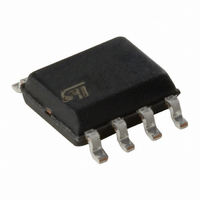
LM2904WD STMicroelectronics, LM2904WD Datasheet

LM2904WD
Specifications of LM2904WD
Available stocks
Related parts for LM2904WD
LM2904WD Summary of contents
Page 1
Features ■ Internally frequency compensated ■ Large DC voltage gain: 100 dB ■ Wide bandwidth (unity gain): 1.1 MHz (temperature compensated) ■ Very low supply current/op (500 µA) ■ Low input bias current (temperature compensated) ■ Low input ...
Page 2
Schematic diagram 1 Schematic diagram Figure 1. Schematic diagram (1/2 LM2904W) 2/20 Doc ID 9893 Rev 9 LM2904W ...
Page 3
LM2904W 2 Absolute maximum ratings and operating conditions Table 1. Absolute maximum ratings (AMR) Symbol (1) V Supply voltage CC V Differential input voltage id V Input voltage in Output short-circuit duration (4) I Input current in T Storage temperature ...
Page 4
Absolute maximum ratings and operating conditions Table 2. Operating conditions Symbol V Supply voltage CC Common mode input voltage range V icm ≤ T ≤ min amb max T Operating free-air temperature range oper 4/20 Parameter Doc ID ...
Page 5
LM2904W 3 Electrical characteristics + - Table 5V Symbol (1) Input offset voltage V io ≤ T ≤ min amb max DV Input offset voltage drift io Input offset current I io ...
Page 6
Electrical characteristics + - Table 5V Symbol Gain bandwidth product GBP + f = 100kHz 30V Total harmonic distortion THD f = 1kHz 20dB ...
Page 7
LM2904W Figure 2. Open loop frequency response 140 0.1 μ F 120 100 30V & -55°C T amb + 15V & -55°C T ...
Page 8
Electrical characteristics Figure 8. Input current versus temperature Figure 10. Input voltage range t V Figure 12. Voltage gain 160 120 POSITIVE SUPPLY VOLTAGE (V) 8/20 Figure ...
Page 9
LM2904W Figure 14. Gain bandwidth product P Figure 16. Common mode rejection ratio P Figure 15. Power supply rejection ratio Figure 17. Phase margin vs capacitive load Phase Margin at Vcc=15V and Vicm=7.5V Vs. Iout and Capacitive load value Doc ...
Page 10
Electrical characteristics Typical single-supply applications Figure 18. AC coupled inverting amplifier Figure 20. Non-inverting DC gain Figure 22. High input Z, DC differential amplifier 10/20 Figure 19. AC coupled non-inverting amplifier Figure 21. DC summing amplifier Figure 23. Using symmetrical ...
Page 11
LM2904W Figure 24. Low drift peak detector Figure 25. Active bandpass filter Doc ID 9893 Rev 9 Electrical characteristics 11/20 ...
Page 12
Macromodel 4 Macromodel 4.1 Important note concerning this macromodel Please consider the following remarks before using this macromodel. ● All models are a trade-off between accuracy and complexity (i.e. simulation time). ● Macromodels are not a substitute to breadboarding; rather, ...
Page 13
LM2904W DINR 15 18 MDTH 400E-12 VIP 4 18 2.000000E+00 FCP 4 5 VOFP 3.400000E+01 FCN 5 4 VOFN 3.400000E+01 FIBP 2 5 VOFN 2.000000E-03 FIBN 5 1 VOFP 2.000000E-03 * AMPLIFYING STAGE FIP 5 19 VOFP 3.600000E+02 FIN 5 ...
Page 14
Package information 5 Package information In order to meet environmental requirements, ST offers these devices in different grades of ® ECOPACK packages, depending on their level of environmental compliance. ECOPACK specifications, grade definitions and product status are available at: www.st.com. ...
Page 15
LM2904W 5.1 SO-8 package information Figure 26. SO-8 package mechanical drawing Table 4. SO-8 package mechanical data Ref ccc Dimensions Millimeters Min. Typ. Max. 1.75 0.10 0.25 ...
Page 16
Package information 5.2 DIP8 package information Figure 27. DIP8 package mechanical drawing Table 5. DIP8 package mechanical data Ref 16/20 Dimensions Millimeters Min. Typ. Max. 5.33 0.38 ...
Page 17
LM2904W 5.3 TSSOP8 package information Figure 28. TSSOP8 package mechanical drawing Table 6. TSSOP8 package mechanical data Ref aaa Dimensions Millimeters Min. Typ. Max. 1.20 0.05 0.15 0.80 ...
Page 18
... Ordering information 6 Ordering information Table 7. Order codes Temperature Order code range LM2904WN LM2904WD LM2904WDT LM2904WPT -40°C, +125°C (1) LM2904WYD (1) LM2904WYDT (2) LM2904WYPT 1. Qualified and characterized according to AEC Q100 and Q003 or equivalent, advanced screening according to AEC Q001 & Q 002 or equivalent. 2. Qualification and characterization according to AEC Q100 and Q003 or equivalent, advanced screening according to AEC Q001 & ...
Page 19
LM2904W 7 Revision history Table 8. Document revision history Date Revision 1-Sep-2003 1 1-Jul-2005 2 1-Oct-2005 3 1-Dec-2005 4 2-May-2006 5 20-Jul-2007 6 18-Dec-2007 7 21-Feb-2008 8 24-Feb-2011 9 Initial release. PPAP references inserted in the datasheet see on page ...
Page 20
... Information in this document is provided solely in connection with ST products. STMicroelectronics NV and its subsidiaries (“ST”) reserve the right to make changes, corrections, modifications or improvements, to this document, and the products and services described herein at any time, without notice. All ST products are sold pursuant to ST’s terms and conditions of sale. ...


