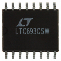
LTC693CSW Linear Technology, LTC693CSW Datasheet

LTC693CSW
Specifications of LTC693CSW
Available stocks
Related parts for LTC693CSW
LTC693CSW Summary of contents
Page 1
... L, LT, LTC, LTM, Linear Technology and the Linear logo are registered trademarks of Linear Technology Corporation. All other trademarks are the property of their respective owners.. V ...
Page 2
LTC692/LTC693 ABSOLUTE MAXIMUM RATINGS Terminal Voltage V ...................................................... –0. ................................................... –0.3V to 6.0V BATT All Other Inputs ..................... –0. Input Current V ................................................................. 200mA CC V ................................................................ 50mA BATT GND ................................................................. 20mA PIN CONFIGURATION ...
Page 3
PRODUCT SELECTION GUIDE RESET THRESHOLD PINS (V) LTC692 8 4.40 LTC693 16 4.40 LTC690 8 4.65 LTC691 16 4.65 LTC694 8 4.65 LTC695 16 4.65 LTC699 8 4.65 LTC1232 8 4.37/4.62 LTC1235 16 4.65 LTC694-3.3 8 2.90 LTC695-3.3 16 2.90 ...
Page 4
LTC692/LTC693 ELECTRICAL CHARACTERISTICS temperature range, otherwise specifi cations are at T PARAMETER Watchdog Timeout Period, Internal Oscillator Watchdog Timeout Period, External Clock (Note 6) Reset Active Time PSRR Watchdog Timeout Period PSRR, Internal OSC Minimum WDI Input Pulse Width RESET ...
Page 5
ELECTRICAL CHARACTERISTICS temperature range, otherwise specifi cations are at T PARAMETER Oscillator OSC IN Input Current (Note 7) OSC SEL Input Pull-Up Current (Note 7) OSC IN Frequency Range OSC IN Frequency with External Capacitor Note 1: Stresses beyond those ...
Page 6
LTC692/LTC693 TYPICAL PERFORMANCE CHARACTERISTICS OUT OUT 5. 2.8V BATT T = 25°C A 4.95 4.90 SLOPE = 5Ω 4.85 4.80 4. LOAD CURRENT (mA) 692_3 • ...
Page 7
PIN FUNCTIONS BATT ON: Battery On Logic Output from Comparator C2. BATT ON goes low when V is internally connected to OUT V . The output typically sinks 35mA and can provide base CC drive for an external PNP transistor ...
Page 8
LTC692/LTC693 PIN FUNCTIONS WDI: Watchdog Input. WDI is a three level input. Driving WDI either high or low for longer than the watchdog timeout period, forces both RESET and WDO low. Floating WDI disables the watchdog timer. The timer resets ...
Page 9
APPLICATIONS INFORMATION Microprocessor Reset The LTC692/LTC693 use a bandgap voltage reference and a precision voltage comparator C1 to monitor the 5V supply input on V (see Block Diagram). When V CC falls below the reset voltage threshold, the RESET output ...
Page 10
LTC692/LTC693 APPLICATIONS INFORMATION ANY PNP POWER TRANSISTOR 5 BATT OUT CC 0.1μF LTC693 1 V BATT GND 3V 4 692_3 • F02 Figure 2. Using BATT ON to Drive External PNP Transistor The LTC692/LTC693 ...
Page 11
APPLICATIONS INFORMATION If battery connections are made through long wires, a 10Ω to 100Ω series resistor and a 0.1μF capacitor are recommended to prevent any overshoot beyond V to the lead inductance (Figure 4). Table 1 shows the state of ...
Page 12
LTC692/LTC693 APPLICATIONS INFORMATION 5V 0.1μF 5V 0.1μF Power-Fail Warning The LTC692/LTC693 generate a power failure output (PFO) for early warning of failure in the microprocessor’s power supply. This is accomplished by comparing the power failure input (PFI) with an internal ...
Page 13
APPLICATIONS INFORMATION V ≥ 7. ≥ 6. Example 1: The circuit in Figure 8 demonstrates the use of the power-fail comparator to monitor the unregulated power supply input. Assuming the the rate of decay of the ...
Page 14
LTC692/LTC693 APPLICATIONS INFORMATION Example 2: The circuit in Figure 9 can be used to measure the regulated 5V supply to provide early warning of power failure. Because of variations in the PFI threshold, this circuit requires adjustment to ensure the ...
Page 15
APPLICATIONS INFORMATION The LTC693 provides an additional output (watchdog output, WDO) which goes low if the watchdog timer is allowed to time out and remains low until set high by the next transition on the WDI pin. WDO is also ...
Page 16
LTC692/LTC693 APPLICATIONS INFORMATION Pushbutton Reset The LTC692/LTC693 do not provide a logic input for direct connection to a pushbutton. However, a pushbutton in series with a 100Ω resistor connected to the RESET output pin (Figure 13) provides an alternative for ...
Page 17
PACKAGE DESCRIPTION .300 – .325 (7.620 – 8.255) .065 (1.651) .008 – .015 TYP (0.203 – 0.381) +.035 .325 –.015 ( ) +0.889 8.255 –0.381 NOTE: INCHES 1. DIMENSIONS ARE MILLIMETERS *THESE DIMENSIONS DO NOT INCLUDE MOLD FLASH OR PROTRUSIONS. ...
Page 18
LTC692/LTC693 PACKAGE DESCRIPTION .300 – .325 .130 ± .005 (7.620 – 8.255) (3.302 ± 0.127) .020 (0.508) MIN .008 – .015 (0.203 – 0.381) +.035 .325 –.015 .120 ( ) +0.889 (3.048) 8.255 –0.381 MIN NOTE: INCHES 1. DIMENSIONS ARE ...
Page 19
... Revised Features section to remove “UL Recognized” and UL logo. Information furnished by Linear Technology Corporation is believed to be accurate and reliable. However, no responsibility is assumed for its use. Linear Technology Corporation makes no representa- tion that the interconnection of its circuits as described herein will not infringe on existing patent rights. ...
Page 20
... MSOP and 3mm × 2mm DFN-10 Packages Manual Reset, 10-Lead MSOP and 3mm × 2mm DFN-10 Packages www.linear.com ● Timing Specifi cations FALL Pin, RST/RST Outputs Pin, Adjustable Reset Timer LT 0310 REV B • PRINTED IN USA © LINEAR TECHNOLOGY CORPORATION 1993 0692fb ...


