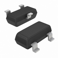
MAX809SN120T1G ON Semiconductor, MAX809SN120T1G Datasheet

MAX809SN120T1G
Specifications of MAX809SN120T1G
Related parts for MAX809SN120T1G
MAX809SN120T1G Summary of contents
Page 1
MAX809 Series, MAX810 Series Very Low Supply Current 3-Pin Microprocessor Reset Monitors The MAX809 and MAX810 are cost−effective system supervisor circuits designed to monitor V in digital systems and provide a reset CC signal to the host processor when necessary. ...
Page 2
Timeout V CC Counter Vref 1 GND Figure 2. MAX809 Series Complementary Active−Low Output 3 Timeout V CC Counter Vref 1 GND Figure 3. MAX810 Series Complementary Active−High Output http://onsemi.com V CC Oscillator V CC Oscillator 2 2 RESET ...
Page 3
PIN DESCRIPTION Pin No. Symbol 1 GND Ground 2 RESET (MAX809) RESET output remains low while V period after V 2 RESET (MAX810) RESET output remains high while V period after Supply Voltage (Typ) CC ABSOLUTE MAXIMUM ...
Page 4
... −40°C to +85° +85°C to +105° Production testing done 25°C, over temperature limits guaranteed by design Contact your ON Semiconductor sales representative for other threshold voltage options −40°C to +105°C unless otherwise noted. Typical values are Symbol http://onsemi.com 4 = +25° ...
Page 5
... SINK SINK SINK 5. Production testing done 25°C, over temperature limits guaranteed by design Contact your ON Semiconductor sales representative for timeout options availability for other threshold voltage options. (continued −40°C to +105°C unless otherwise noted. Typical values are at A Symbol http://onsemi ...
Page 6
TYPICAL OPERATING CHARACTERISTICS 0 1 0.5 0.4 0.3 0.2 0.1 0 0.5 1.5 2.5 3.5 SUPPLY VOLTAGE (V) Figure 4. Supply Current vs. Supply Voltage 0. 2. 0.30 0.25 0.20 0.15 0.10 ...
Page 7
TYPICAL OPERATING CHARACTERISTICS SINK RESET ASSERTED 20 85°C 15 25°C 10 −40°C 5.0 0 0.5 1.0 1.5 2.0 2.5 3.0 SUPPLY VOLTAGE (V) Figure 10. Output Voltage Low vs. Supply Voltage 125 ...
Page 8
Detail Operation Description The MAX809/810 series microprocessor supervisory circuits are designed to monitor the power supplies in digital systems and provide a reset signal to the processor without any external components. Figure 2 shows the timing diagram and a typical ...
Page 9
V Transient Rejection CC The MAX809 provides accurate V reset timing during power−up, power−down, and brownout/sag conditions, and rejects negative−going transients (glitches) on the power supply line. Figure 16 shows the maximum transient duration vs. maximum negative excursion (overdrive) for ...
Page 10
... MAX809JTRG 4.00 MAX809MTR 4.38 MAX809MTRG 4.38 MAX809HTR 4.55 MAX809HTRG 4.55 MAX809LTR 4.63 MAX809LTRG 4.63 NCV809LTRG 4.63 MAX809SN490T1 4.90 MAX809SN490T1G 4.90 MAX809SN120T1G 1.20 MAX809SN293D1T1G 2.93 MAX809SN293D2T1G 2.93 MAX809SN293D3T1G 2.93 MAX809SQ120T1G 1.20 MAX809SQ232T1G 2.32 MAX809SQ263T1G 2.63 MAX809SQ293T1G 2.93 MAX809SQ308T1G 3.08 MAX809SQ400T1G 4.00 MAX809SQ438T1G 4 ...
Page 11
... MAX810SQ293D2T1G 2.93 MAX810SQ293D3T1G 2.93 †For information on tape and reel specifications,including part orientation and tape sizes, please refer to our Tape and Reel Packaging Specifications Brochure, BRD8011/D. *Contact your ON Semiconductor sales representative for other threshold voltage options. Timeout* Description Marking (ms) 140−460 140−460 140− ...
Page 12
... *For additional information on our Pb−Free strategy and soldering details, please download the ON Semiconductor Soldering and Mounting Techniques Reference Manual, SOLDERRM/D. PACKAGE DIMENSIONS SOT−23 (TO236) CASE 318−08 ISSUE AN NOTES: 1. DIMENSIONING AND TOLERANCING PER ANSI Y14.5M, 1982. 2. CONTROLLING DIMENSION: INCH. 3. MAXIMUM LEAD THICKNESS INCLUDES LEAD FINISH THICKNESS ...
Page 13
... A1 *For additional information on our Pb−Free strategy and soldering details, please download the ON Semiconductor Soldering and Mounting Techniques Reference Manual, SOLDERRM/D. ON Semiconductor and are registered trademarks of Semiconductor Components Industries, LLC (SCILLC). SCILLC reserves the right to make changes without further notice to any products herein ...


