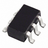
ADP3330ARTZ3.3-RL7 Analog Devices Inc, ADP3330ARTZ3.3-RL7 Datasheet - Page 2

ADP3330ARTZ3.3-RL7
Manufacturer Part Number
ADP3330ARTZ3.3-RL7
Description
IC REG LDO 200MA 3.3V SOT23-6
Manufacturer
Analog Devices Inc
Series
anyCAP®r
Type
Linearr
Datasheet
1.ADP3330ARTZ3.3-RL7.pdf
(12 pages)
Specifications of ADP3330ARTZ3.3-RL7
Design Resources
Half-Duplex, Isolated RS-485 Interface (CN0031) USB Hub Isolator Circuit (CN0158)
Regulator Topology
Positive Fixed
Voltage - Output
3.3V
Voltage - Input
Up to 12V
Voltage - Dropout (typical)
0.14V @ 200mA
Number Of Regulators
1
Current - Output
200mA
Operating Temperature
-40°C ~ 85°C
Mounting Type
Surface Mount
Package / Case
SOT-23-6
Primary Input Voltage
12V
Output Voltage Fixed
3.3V
Dropout Voltage Vdo
140mV
No. Of Pins
6
Output Current
200mA
Operating Temperature Range
-40°C To +85°C
Msl
MSL 3 - 168 Hours
Package
6SOT-23
Function
LDO
Number Of Outputs
1
Input Voltage Range
12 to 2.9 V
Output Voltage
3.3 V
Maximum Output Current
0.3(Typ) A
Output Type
Fixed
Accuracy
±0.7 %
Typical Dropout Voltage @ Current
0.14@200mA|0.025@1mA|0.11@150mA|0.042@10mA V
Polarity
Positive
Lead Free Status / RoHS Status
Lead free / RoHS Compliant
Current - Limit (min)
-
Lead Free Status / RoHS Status
Lead free / RoHS Compliant, Lead free / RoHS Compliant
Other names
ADP3330ARTZ3.3-RL7TR
Available stocks
Company
Part Number
Manufacturer
Quantity
Price
Part Number:
ADP3330ARTZ3.3-RL7
Manufacturer:
ADI/亚德诺
Quantity:
20 000
unless otherwise noted).
ADP3330-xx–SPECIFICATIONS
Parameter
OUTPUT VOLTAGE ACCURACY
LINE REGULATION
LOAD REGULATION
GROUND CURRENT
GROUND CURRENT IN DROPOUT
DROPOUT VOLTAGE
PEAK LOAD CURRENT
OUTPUT NOISE
SHUTDOWN THRESHOLD
SHUTDOWN PIN INPUT CURRENT
GROUND CURRENT IN SHUTDOWN
OUTPUT CURRENT IN SHUTDOWN
ERROR PIN OUTPUT LEAKAGE
ERROR PIN OUTPUT “LOW”
NOTES
1
2
3
Specifications subject to change without notice.
Ambient temperature of +85 C corresponds to a junction temperature of +125 C under typical full load test conditions.
Application stable with no load.
See detail in Figure 19 and Application section of data sheet.
MODE
MODE
VOLTAGE
3
1, 2
The following specifications apply to all voltage options except –2.5.
Symbol
V
I
I
V
I
V
V
I
I
I
I
V
GND
GND
LDPK
SD
GNDSD
OSD
EL
V
V
OUT
DROP
NOISE
THSD
EOL
I
V
L
O
IN
O
Conditions
V
I
T
V
I
T
V
I
T
V
T
I
T
I
I
I
I
V
I
V
I
I
I
I
V
f = 10 Hz–100 kHz, C
I
f = 10 Hz–100 kHz, C
I
ON
OFF
V
0 < SD,
SD = 0 V, V
T
T
V
I
L
L
L
L
L
L
L
L
L
L
L
L
L
L
L
SINK
IN
IN
IN
IN
IN
OUT
IN
IN
EO
A
A
A
A
A
A
A
= 200 mA, C
= 200 mA, C
= 0.1 mA to 200 mA
= 0.1 mA to 150 mA
= 0.1 mA to 200 mA
= 0.1 mA to 200 mA
= 200 mA, T
= 150 mA
= 50 mA
= 0.1 mA
= 0.1 mA
= 200 mA, T
= 150 mA
= 10 mA
= 1 mA
= –40 C to +85 C
= –20 C to +85 C
= +25 C
= +25 C
= +25 C
= +25 C @ V
= +85 C @ V
= V
= V
= V
= V
= V
= V
= 12 V, 0 < SD,
= 5 V
= 400 A
= 98% of V
(@ T
OUTNOM
OUTNOM
OUTNOM
OUTNOM
OUTNOM
OUTNOM
–2–
5 V
A
IN
= –40 C to +85 C, V
= 12 V
NR
NR
A
A
+0.25 V to +12 V
+0.25 V to +12 V
+0.25 V to +12 V
+0.25 V to +12 V
– 100 mV
+ 1 V
= –20 C to +85 C
IN
IN
OUTNOM
= –20 C to +85 C
= 10 nF, V
= 0 nF, V
= 12 V
= 12 V
L
L
12 V
= 10 F
= 10 F
OUT
OUT
= 3 V
= 3 V
IN
= +7 V, C
Min
–0.7
–1.4
–1.4
2.0
IN
= 0.47 F, C
Typ
0.04
0.04
1.6
1.2
0.4
34
37
0.14
0.11
0.042
0.025
300
47
95
1.9
1.4
0.01
0.19
OUT
= 0.47 F,
Max
+0.7
+1.4
+1.4
4.0
3.1
1.1
50
55
0.23
0.17
0.06
0.05
0.4
9
6
2
1
2
1
0.40
2
REV. A
Units
%
%
%
mV/V
mV/mA
mA
mA
mA
V
V
V
V
mA
V
V
V
V rms
V rms
A
A
A
A
A
A
A
A


